DatasheetsDatasheet MCP6241, MCP6241R, MCP6241U, …
Datasheet MCP6241, MCP6241R, MCP6241U, MCP62412, MCP62414 (Microchip)
| Производитель | Microchip |
| Описание | MCP6241/1R/1U/2/4 family of operational amplifier (Op Amp) provides wide bandwidth for the quiescent current |
| Страниц / Страница | 38 / 1 — MCP6241/1R/1U/2/4. 50 µA, 550 kHz Rail-to-Rail Op Amp. Features. … |
| Формат / Размер файла | PDF / 684 Кб |
| Язык документа | английский |
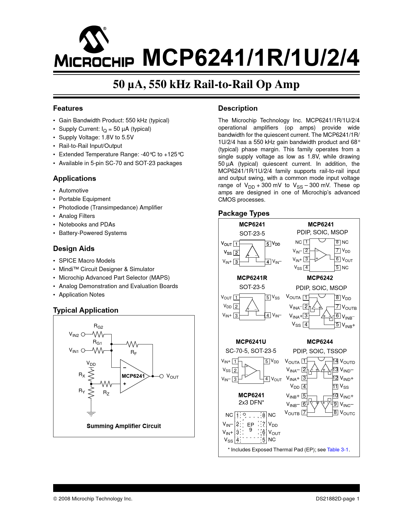
MCP6241/1R/1U/2/4. 50 µA, 550 kHz Rail-to-Rail Op Amp. Features. Description. Applications. Package Types. MCP6241. Design Aids
Модельный ряд для этого даташита
Текстовая версия документа
link to page 9
MCP6241/1R/1U/2/4 50 µA, 550 kHz Rail-to-Rail Op Amp Features Description
• Gain Bandwidth Product: 550 kHz (typical) The Microchip Technology Inc. MCP6241/1R/1U/2/4 • Supply Current: I operational amplifiers (op amps) provide wide Q = 50 µA (typical) • Supply Voltage: 1.8V to 5.5V bandwidth for the quiescent current. The MCP6241/1R/ 1U/2/4 has a 550 kHz gain bandwidth product and 68° • Rail-to-Rail Input/Output (typical) phase margin. This family operates from a • Extended Temperature Range: -40°C to +125°C single supply voltage as low as 1.8V, while drawing • Available in 5-pin SC-70 and SOT-23 packages 50 µA (typical) quiescent current. In addition, the MCP6241/1R/1U/2/4 family supports rail-to-rail input
Applications
and output swing, with a common mode input voltage range of VDD + 300 mV to VSS – 300 mV. These op • Automotive amps are designed in one of Microchip’s advanced • Portable Equipment CMOS processes. • Photodiode (Transimpedance) Amplifier
Package Types
• Analog Filters • Notebooks and PDAs
MCP6241 MCP6241
• Battery-Powered Systems SOT-23-5 PDIP, SOIC, MSOP V NC 1 8 NC OU V T OU 1 5 V 5
Design Aids
DD V V 2 – 7 VDD SS 2 + IN– – • SPICE Macro Models 3 + 6 V VIN+ VOUT IN+ 3 4 VIN– • Mindi™ Circuit Designer & Simulator VSS 4 5 NC • Microchip Advanced Part Selector (MAPS)
MCP6241R MCP6242
• Analog Demonstration and Evaluation Boards SOT-23-5 PDIP, SOIC, MSOP • Application Notes V V OUT 1 5 VSS OUTA 1 8 VDD V _
Typical Application
DD 2 + V 2 INA - + 7 V – OUTB VIN+ 3 4 VIN– V 3 + _ INA+ - 6 VINB R VSS 4 5 V G2 INB+ VIN2 R
MCP6241U MCP6244
G1 VIN1 R SC-70-5, SOT-23-5 PDIP, SOIC, TSSOP F V VIN+ 1 5 VDD V 1 14 V DD + OUTA OUTD
–
VSS 2 VINA– 2 - + + - 13 VIND– RX
MCP6241
V – OUT V V 3 12 V IN– 3 4 VOUT INA+ IND+
+
VDD 4 11 VSS RY RZ
MCP6241
V 5 10 INB+ VINC+ 2x3 DFN* V 6 - + + - 9 INB– VINC– V 7 8 OUTB VOUTC NC 1 8 NC
Summing Amplifier Circuit
VIN– 2 EP 7 VDD V 9 IN+ 3 6 VOUT VSS 4 5 NC * Includes Exposed Thermal Pad (EP); see Table 3-1. © 2008 Microchip Technology Inc. DS21882D-page 1 Document Outline 1.0 Electrical Characteristics 1.1 Test Circuits FIGURE 1-1: AC and DC Test Circuit for Most Non-Inverting Gain Conditions. FIGURE 1-2: AC and DC Test Circuit for Most Inverting Gain Conditions. 2.0 Typical Performance Curves FIGURE 2-1: Input Offset Voltage. FIGURE 2-2: PSRR, CMRR vs. Frequency. FIGURE 2-3: Input Bias Current at +85˚C. FIGURE 2-4: CMRR, PSRR vs. Ambient Temperature. FIGURE 2-5: Open-Loop Gain, Phase vs. Frequency. FIGURE 2-6: Input Bias Current at +125˚C. FIGURE 2-7: Input Noise Voltage Density vs. Frequency. FIGURE 2-8: Input Offset Voltage vs. Common Mode Input Voltage at VDD = 1.8V. FIGURE 2-9: Input Offset Voltage vs. Common Mode Input Voltage at VDD = 5.5V. FIGURE 2-10: Input Offset Voltage Drift. FIGURE 2-11: Input Offset Voltage vs. Output Voltage. FIGURE 2-12: Output Short-Circuit Current vs. Ambient Temperature. FIGURE 2-13: Slew Rate vs. Ambient Temperature. FIGURE 2-14: Output Voltage Headroom vs. Output Current Magnitude. FIGURE 2-15: Maximum Output Voltage Swing vs. Frequency. FIGURE 2-16: Small-Signal, Non-Inverting Pulse Response. FIGURE 2-17: Large-Signal, Non-Inverting Pulse Response. FIGURE 2-18: Quiescent Current vs. Power Supply Voltage. FIGURE 2-19: Measured Input Current vs. Input Voltage (below VSS). 3.0 Pin Descriptions TABLE 3-1: Pin Function Table for Single Op Amps TABLE 3-2: Pin Function Table for Dual and Quad Op Amps 3.1 Analog Outputs 3.2 Analog Inputs 3.3 Power Supply (VSS and VDD) 3.4 Exposed Thermal Pad (EP) 4.0 Application infoRmation 4.1 Rail-to-Rail Inputs FIGURE 4-1: The MCP6241/1R/1U/2/4 Show No Phase Reversal. FIGURE 4-2: Simplified Analog Input ESD Structures. FIGURE 4-3: Protecting the Analog Inputs. 4.2 Rail-to-Rail Output 4.3 Capacitive Loads FIGURE 4-4: Output Resistor, RISO stabilizes large capacitive loads. FIGURE 4-5: Recommended RISO Values for Capacitive Loads. 4.4 Supply Bypass 4.5 Unused Op Amps FIGURE 4-6: Unused Op Amps. 4.6 PCB Surface Leakage FIGURE 4-7: Example Guard Ring Layout for Inverting Gain. 4.7 Application Circuits FIGURE 4-8: Summing Amplifier Circuit. FIGURE 4-9: Effect of Parasitic Capacitance at the Input. 5.0 Design AIDS 5.1 SPICE Macro Model 5.2 Mindi™ Circuit Designer & Simulator 5.3 Microchip Advanced Part Selector (MAPS) 5.4 Analog Demonstration and Evaluation Boards 5.5 Application Notes 6.0 Packaging Information 6.1 Package Marking Information

 аккумуляторов")


