DatasheetsDatasheet MCP6001, MCP6001R, MCP6001U, …
Datasheet MCP6001, MCP6001R, MCP6001U, MCP6002, MCP6004 (Microchip)
| Производитель | Microchip |
| Описание | The MCP6001 is a single general purpose op amp offering rail-to-rail input and output over the 1.8 to 6V operating range |
| Страниц / Страница | 42 / 1 — MCP6001/1R/1U/2/4. 1 MHz, Low-Power Op Amp. Features. Description. … |
| Формат / Размер файла | PDF / 794 Кб |
| Язык документа | английский |
MCP6001/1R/1U/2/4. 1 MHz, Low-Power Op Amp. Features. Description. Applications. Package Types. MCP6001. MCP6001R. Design Aids. MCP6002
Модельный ряд для этого даташита
Текстовая версия документа
link to page 11
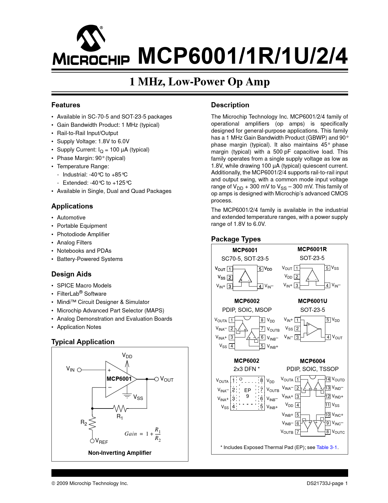
MCP6001/1R/1U/2/4 1 MHz, Low-Power Op Amp Features Description
• Available in SC-70-5 and SOT-23-5 packages The Microchip Technology Inc. MCP6001/2/4 family of • Gain Bandwidth Product: 1 MHz (typical) operational amplifiers (op amps) is specifically • Rail-to-Rail Input/Output designed for general-purpose applications. This family has a 1 MHz Gain Bandwidth Product (GBWP) and 90° • Supply Voltage: 1.8V to 6.0V phase margin (typical). It also maintains 45° phase • Supply Current: IQ = 100 µA (typical) margin (typical) with a 500 pF capacitive load. This • Phase Margin: 90° (typical) family operates from a single supply voltage as low as • Temperature Range: 1.8V, while drawing 100 µA (typical) quiescent current. - Industrial: -40°C to +85°C Additionally, the MCP6001/2/4 supports rail-to-rail input and output swing, with a common mode input voltage - Extended: -40°C to +125°C range of VDD + 300 mV to VSS – 300 mV. This family of • Available in Single, Dual and Quad Packages op amps is designed with Microchip’s advanced CMOS process.
Applications
The MCP6001/2/4 family is available in the industrial • Automotive and extended temperature ranges, with a power supply • Portable Equipment range of 1.8V to 6.0V. • Photodiode Amplifier
Package Types
• Analog Filters • Notebooks and PDAs
MCP6001 MCP6001R
• Battery-Powered Systems SC70-5, SOT-23-5 SOT-23-5 V V VOUT 1 5 V OUT OU 1 5 V 5 DD SS
Design Aids
V V SS 2 + DD 2 + - - • SPICE Macro Models V 3 4 V VIN+ 3 4 V IN+ 3 4 IN– IN– • FilterLab® Software • Mindi™ Circuit Designer & Simulator
MCP6002 MCP6001U
• Microchip Advanced Part Selector (MAPS) PDIP, SOIC, MSOP SOT-23-5 • Analog Demonstration and Evaluation Boards V V V OUTA 1 8 V IN+ 1 5 DD DD + • Application Notes VINA– 2 - + 7 V V OUTB SS 2 - V 3 + - 6 V VIN– 3 4 V
Typical Application
INA+ INB– OUT VSS 4 5 VINB+ VDD
MCP6002 MCP6004
VIN + 2x3 DFN * PDIP, SOIC, TSSOP
MCP6001
VOUT V VOUTA 1 8 V OUTA 1 14 VOUTD DD – VINA– 2 2 EP 7 V - + + - 13 VIND– VINA– OUTB V 9 V 12 V SS INA+ 3 IND+ VINA+ 3 6 VINB– VDD 4 11 VSS VSS 4 5 VINB+ R VINB+ 5 10 VINC+ 1 R - + - 2 V + INB– 6 9 VINC– R V V Gain = 1 1 + --- OUTB 7 8 OUTC R V 2 REF * Includes Exposed Thermal Pad (EP); see Table 3-1.
Non-Inverting Amplifier
© 2009 Microchip Technology Inc. DS21733J-page 1 Document Outline 1.0 Electrical Characteristics 1.1 Test Circuits FIGURE 1-1: AC and DC Test Circuit for Most Specifications. 2.0 Typical Performance Curves FIGURE 2-1: Input Offset Voltage. FIGURE 2-2: Input Offset Voltage Drift. FIGURE 2-3: Input Offset Quadratic Temp. Co. FIGURE 2-4: Input Offset Voltage vs. Common Mode Input Voltage at VDD = 1.8V. FIGURE 2-5: Input Offset Voltage vs. Common Mode Input Voltage at VDD = 5.5V. FIGURE 2-6: Input Offset Voltage vs. Output Voltage. FIGURE 2-7: Input Bias Current at +85°C. FIGURE 2-8: Input Bias Current at +125°C. FIGURE 2-9: CMRR, PSRR vs. Ambient Temperature. FIGURE 2-10: PSRR, CMRR vs. Frequency. FIGURE 2-11: Open-Loop Gain, Phase vs. Frequency. FIGURE 2-12: Input Noise Voltage Density vs. Frequency. FIGURE 2-13: Output Short Circuit Current vs. Power Supply Voltage. FIGURE 2-14: Output Voltage Headroom vs. Output Current Magnitude. FIGURE 2-15: Quiescent Current vs. Power Supply Voltage. FIGURE 2-16: Small-Signal, Non-Inverting Pulse Response. FIGURE 2-17: Large-Signal, Non-Inverting Pulse Response. FIGURE 2-18: Slew Rate vs. Ambient Temperature. FIGURE 2-19: Output Voltage Swing vs. Frequency. FIGURE 2-20: Measured Input Current vs. Input Voltage (below VSS). FIGURE 2-21: The MCP6001/2/4 Show No Phase Reversal. 3.0 Pin Descriptions TABLE 3-1: Pin Function Table 3.1 Analog Outputs 3.2 Analog Inputs 3.3 Power Supply Pins 3.4 Exposed Thermal Pad (EP) 4.0 Application Information 4.1 Rail-to-Rail Inputs FIGURE 4-1: Simplified Analog Input ESD Structures. FIGURE 4-2: Protecting the Analog Inputs. 4.2 Rail-to-Rail Output 4.3 Capacitive Loads FIGURE 4-3: Output resistor, RISO stabilizes large capacitive loads. FIGURE 4-4: Recommended RISO values for Capacitive Loads. 4.4 Supply Bypass 4.5 Unused Op Amps FIGURE 4-5: Unused Op Amps. 4.6 PCB Surface Leakage FIGURE 4-6: Example Guard Ring Layout for Inverting Gain. 4.7 Application Circuits FIGURE 4-7: Instrumentation Amplifier with Unity-Gain Buffer Inputs. FIGURE 4-8: Active Second-Order Low-Pass Filter. FIGURE 4-9: Peak Detector with Clear and Sample CMOS Analog Switches. 5.0 Design AIDS 5.1 SPICE Macro Model 5.2 FilterLab® Software 5.3 Mindi™ Circuit Designer & Simulator 5.4 Microchip Advanced Part Selector (MAPS) 5.5 Analog Demonstration and Evaluation Boards 5.6 Application Notes 6.0 Packaging Information 6.1 Package Marking Information

 аккумуляторов")


