DatasheetsDatasheet ADA4096-2, ADA4096-4 (Analog …
Datasheet ADA4096-2, ADA4096-4 (Analog Devices)
| Производитель | Analog Devices |
| Описание | 30 V, Micropower, Overvoltage Protection, Rail-to-Rail Input/Output Quad Op Amplifier |
| Страниц / Страница | 24 / 1 — 30 V, Micropower, Overvoltage Protection,. Rail-to-Rail Input/Output … |
| Версия | G |
| Формат / Размер файла | PDF / 676 Кб |
| Язык документа | английский |
30 V, Micropower, Overvoltage Protection,. Rail-to-Rail Input/Output Amplifiers. Data Sheet. ADA4096-2/. ADA4096-4. FEATURES
Текстовая версия документа
link to page 7 link to page 7 link to page 1
30 V, Micropower, Overvoltage Protection, Rail-to-Rail Input/Output Amplifiers Data Sheet ADA4096-2/ ADA4096-4 FEATURES PIN CONNECTION DIAGRAMS Input overvoltage protection, 32 V above and below the OUTA 1 8 V+ supply rails –INA 2 7 OUTB ADA4096-2 No phase reversal for input voltage up to ±32 V beyond the +INA 3 TOP VIEW 6 –INB (Not to Scale)
001
power supply V– 4 5 +INB
09241-
Rail-to-rail input and output swing
Figure 1. 8-Lead, MSOP (RM-8), ADA4096-2
Low power: 60 µA per amplifier typical Unity-gain bandwidth OUTA 1 8 V+ 800 kHz typical at VSY = ±15 V ADA4096-2 –INA 2 7 OUTB 550 kHz typical at V TOP VIEW SY = ±5 V +INA 3 (Not to Scale) 6 –INB 465 kHz typical at VSY = ±1.5 V V– 4 5 +INB Single-supply operation: 3 V to 30 V Low offset voltage: 300 µV maximum NOTES
002
1. CONNECT THE EXPOSED PAD Large signal voltage gain: 120 dB typical TO V–.
09241-
Unity gain stable
Figure 2. 8-Lead LFCSP (CP-8-10), ADA4096-2
Qualified for automotive applications APPLICATIONS
Note: For the ADA4096-4, see the Pin Configurations and
Battery monitoring
Function Descriptions section.
Sensor conditioners Portable power supply controls Portable instrumentation GENERAL DESCRIPTION T
The ADA4096-2 dual and ADA4096-4 quad operational amplifiers feature micropower operation and rail-to-rail input and output ranges. The extremely low power requirements and guaranteed operation from 3 V to 30 V make these amplifiers perfectly suited to monitor battery usage and to control battery
1
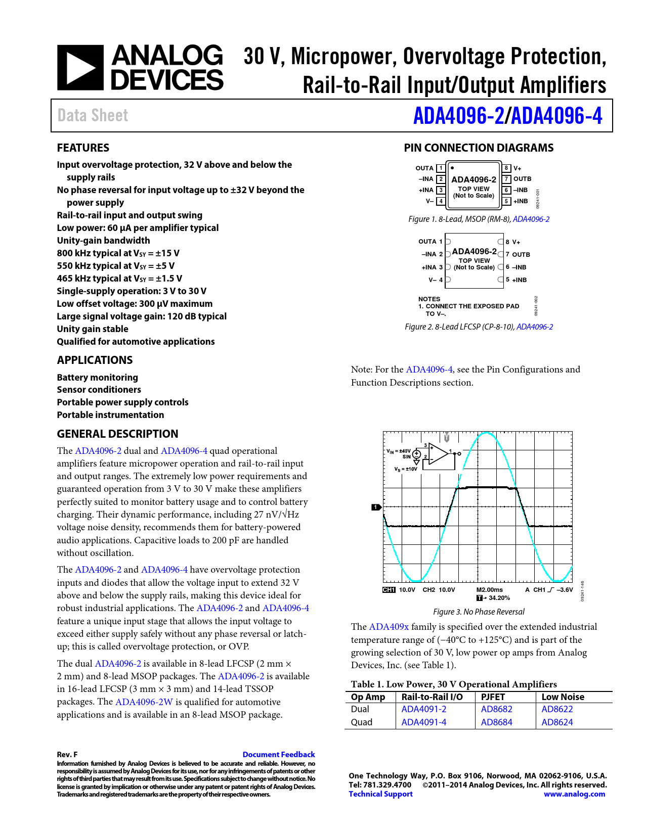
charging. Their dynamic performance, including 27 nV/√Hz voltage noise density, recommends them for battery-powered audio applications. Capacitive loads to 200 pF are handled without oscil ation. The ADA4096-2 and ADA4096-4 have overvoltage protection inputs and diodes that al ow the voltage input to extend 32 V 146 above and below the supply rails, making this device ideal for
CH1 10.0V CH2 10.0V M2.00ms A CH1 –3.6V T 34.20%
09241- robust industrial applications. The ADA4096-2 and ADA4096-4 Figure 3. No Phase Reversal feature a unique input stage that al ows the input voltage to The ADA409x family is specified over the extended industrial exceed either supply safely without any phase reversal or latch- temperature range of (−40°C to +125°C) and is part of the up; this is called overvoltage protection, or OVP. growing selection of 30 V, low power op amps from Analog The dual ADA4096-2 is available in 8-lead LFCSP (2 mm × Devices, Inc. (see Table 1). 2 mm) and 8-lead MSOP packages. The ADA4096-2 is available in 16-lead LFCSP (3 mm × 3 mm) and 14-lead TSSOP
Table 1. Low Power, 30 V Operational Amplifiers
packages. The ADA4096-2W is qualified for automotive
Op Amp Rail-to-Rail I/O PJFET Low Noise
applications and is available in an 8-lead MSOP package. Dual ADA4091-2 AD8682 AD8622 Quad ADA4091-4 AD8684 AD8624
Rev. F Document Feedback Information furnished by Analog Devices is believed to be accurate and reliable. However, no responsibility is assumed by Analog Devices for its use, nor for any infringements of patents or other rights of third parties that may result from its use. Specifications subject to change without notice. No One Technology Way, P.O. Box 9106, Norwood, MA 02062-9106, U.S.A. license is granted by implication or otherwise under any patent or patent rights of Analog Devices. Tel: 781.329.4700 ©2011–2014 Analog Devices, Inc. All rights reserved. Trademarks and registered trademarks are the property of their respective owners. Technical Support www.analog.com
Document Outline FEATURES APPLICATIONS PIN CONNECTION DIAGRAMS GENERAL DESCRIPTION TABLE OF CONTENTS REVISION HISTORY SPECIFICATIONS ELECTRICAL SPECIFICATIONS, VSY = ±1.5 V ELECTRICAL SPECIFICATIONS, VSY = ±5 V ELECTRICAL SPECIFICATIONS, VSY = ±15 V ABSOLUTE MAXIMUM RATINGS THERMAL RESISTANCE ESD CAUTION PIN CONFIGURATIONS AND FUNCTION DESCRIPTIONS TYPICAL PERFORMANCE CHARACTERISTICS ±1.5 V CHARACTERISTICS ±5 V CHARACTERISTICS ±15 V CHARACTERISTICS COMPARATIVE VOLTAGE AND VARIABLE VOLTAGE GRAPHS THEORY OF OPERATION INPUT STAGE PHASE INVERSION INPUT OVERVOLTAGE PROTECTION COMPARATOR OPERATION OUTLINE DIMENSIONS ORDERING GUIDE AUTOMOTIVE PRODUCTS

 аккумуляторов")


