Datasheet AD7780 (Analog Devices)
| Производитель | Analog Devices |
| Описание | 24-Bit Pin-Programmable Low Power Σ−Δ ADC |
| Страниц / Страница | 17 / 1 — 24-Bit, Pin-Programmable,. Ultralow Power Sigma-Delta ADC. AD7780. … |
| Версия | A |
| Формат / Размер файла | PDF / 359 Кб |
| Язык документа | английский |
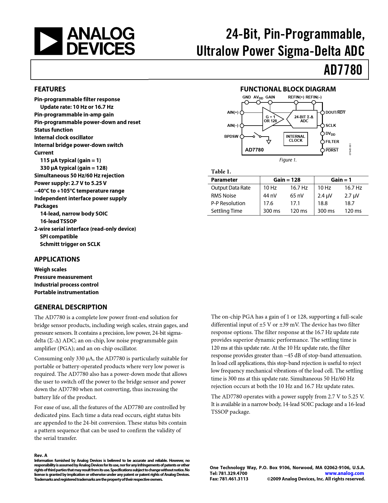
24-Bit, Pin-Programmable,. Ultralow Power Sigma-Delta ADC. AD7780. FEATURES. FUNCTIONAL BLOCK DIAGRAM. GND AV. GAIN
Модельный ряд для этого даташита
Текстовая версия документа
24-Bit, Pin-Programmable, Ultralow Power Sigma-Delta ADC AD7780 FEATURES FUNCTIONAL BLOCK DIAGRAM GND AV GAIN REFIN(+) REFIN(–) Pin-programmable filter response DD Update rate: 10 Hz or 16.7 Hz AIN(+) DOUT/RDY Pin-programmable in-amp gain G = 1 24-BIT Σ-Δ Pin-programmable power-down and reset OR 128 ADC AIN(–) SCLK Status function DVDD Internal clock oscillator BPDSW INTERNAL CLOCK FILTER Internal bridge power-down switch
1
AD7780
-00
PDRST Current
945 07
115 μA typical (gain = 1)
Figure 1.
330 μA typical (gain = 128) Table 1. Simultaneous 50 Hz/60 Hz rejection Parameter Gain = 128 Gain = 1 Power supply: 2.7 V to 5.25 V
Output Data Rate 10 Hz 16.7 Hz 10 Hz 16.7 Hz
−40°C to +105°C temperature range
RMS Noise 44 nV 65 nV 2.4 μV 2.7 μV
Independent interface power supply
P-P Resolution 17.6 17.1 18.8 18.7
Packages
Settling Time 300 ms 120 ms 300 ms 120 ms
14-lead, narrow body SOIC 16-lead TSSOP 2-wire serial interface (read-only device) SPI compatible Schmitt trigger on SCLK APPLICATIONS Weigh scales Pressure measurement Industrial process control Portable instrumentation GENERAL DESCRIPTION
The AD7780 is a complete low power front-end solution for The on-chip PGA has a gain of 1 or 128, supporting a full-scale bridge sensor products, including weigh scales, strain gages, and differential input of ±5 V or ±39 mV. The device has two filter pressure sensors. It contains a precision, low power, 24-bit sigma- response options. The filter response at the 16.7 Hz update rate delta (Σ-Δ) ADC; an on-chip, low noise programmable gain provides superior dynamic performance. The settling time is amplifier (PGA); and an on-chip oscillator. 120 ms at this update rate. At the 10 Hz update rate, the filter response provides greater than −45 dB of stop-band attenuation. Consuming only 330 μA, the AD7780 is particularly suitable for In load cell applications, this stop-band rejection is useful to reject portable or battery-operated products where very low power is low frequency mechanical vibrations of the load cell. The settling required. The AD7780 also has a power-down mode that allows time is 300 ms at this update rate. Simultaneous 50 Hz/60 Hz the user to switch off the power to the bridge sensor and power rejection occurs at both the 10 Hz and 16.7 Hz update rates. down the AD7780 when not converting, thus increasing the battery life of the product. The AD7780 operates with a power supply from 2.7 V to 5.25 V. It is available in a narrow body, 14-lead SOIC package and a 16-lead For ease of use, all the features of the AD7780 are controlled by TSSOP package. dedicated pins. Each time a data read occurs, eight status bits are appended to the 24-bit conversion. These status bits contain a pattern sequence that can be used to confirm the validity of the serial transfer.
Rev. A Information furnished by Analog Devices is believed to be accurate and reliable. However, no responsibility is assumed by Analog Devices for its use, nor for any infringements of patents or other One Technology Way, P.O. Box 9106, Norwood, MA 02062-9106, U.S.A. rights of third parties that may result from its use. Specifications subject to change without notice. No license is granted by implication or otherwise under any patent or patent rights of Analog Devices. Tel: 781.329.4700 www.analog.com Trademarks and registered trademarks are the property of their respective owners. Fax: 781.461.3113 ©2009 Analog Devices, Inc. All rights reserved.
Document Outline FEATURES APPLICATIONS FUNCTIONAL BLOCK DIAGRAM GENERAL DESCRIPTION TABLE OF CONTENTS REVISION HISTORY SPECIFICATIONS TIMING CHARACTERISTICS Circuit and Timing Diagrams ABSOLUTE MAXIMUM RATINGS THERMAL RESISTANCE ESD CAUTION PIN CONFIGURATIONS AND FUNCTION DESCRIPTIONS TYPICAL PERFORMANCE CHARACTERISTICS OUTPUT NOISE AND RESOLUTION THEORY OF OPERATION FILTER, DATA RATE, AND SETTLING TIME GAIN POWER-DOWN/RESET () ANALOG INPUT CHANNEL BIPOLAR CONFIGURATION DATA OUTPUT CODING REFERENCE BRIDGE POWER-DOWN SWITCH DIGITAL INTERFACE APPLICATIONS INFORMATION WEIGH SCALES PERFORMANCE IN A WEIGH SCALE SYSTEM EMI RECOMMENDATIONS GROUNDING AND LAYOUT OUTLINE DIMENSIONS ORDERING GUIDE

 аккумуляторов")


