Datasheet AD7631 (Analog Devices)
| Производитель | Analog Devices |
| Описание | 18-Bit, 250 kSPS, Differential Programmable Input PulSAR® ADC |
| Страниц / Страница | 33 / 1 — 18-Bit, 250 kSPS, Differential. Programmable Input PulSAR® ADC. Data … |
| Версия | B |
| Формат / Размер файла | PDF / 674 Кб |
| Язык документа | английский |
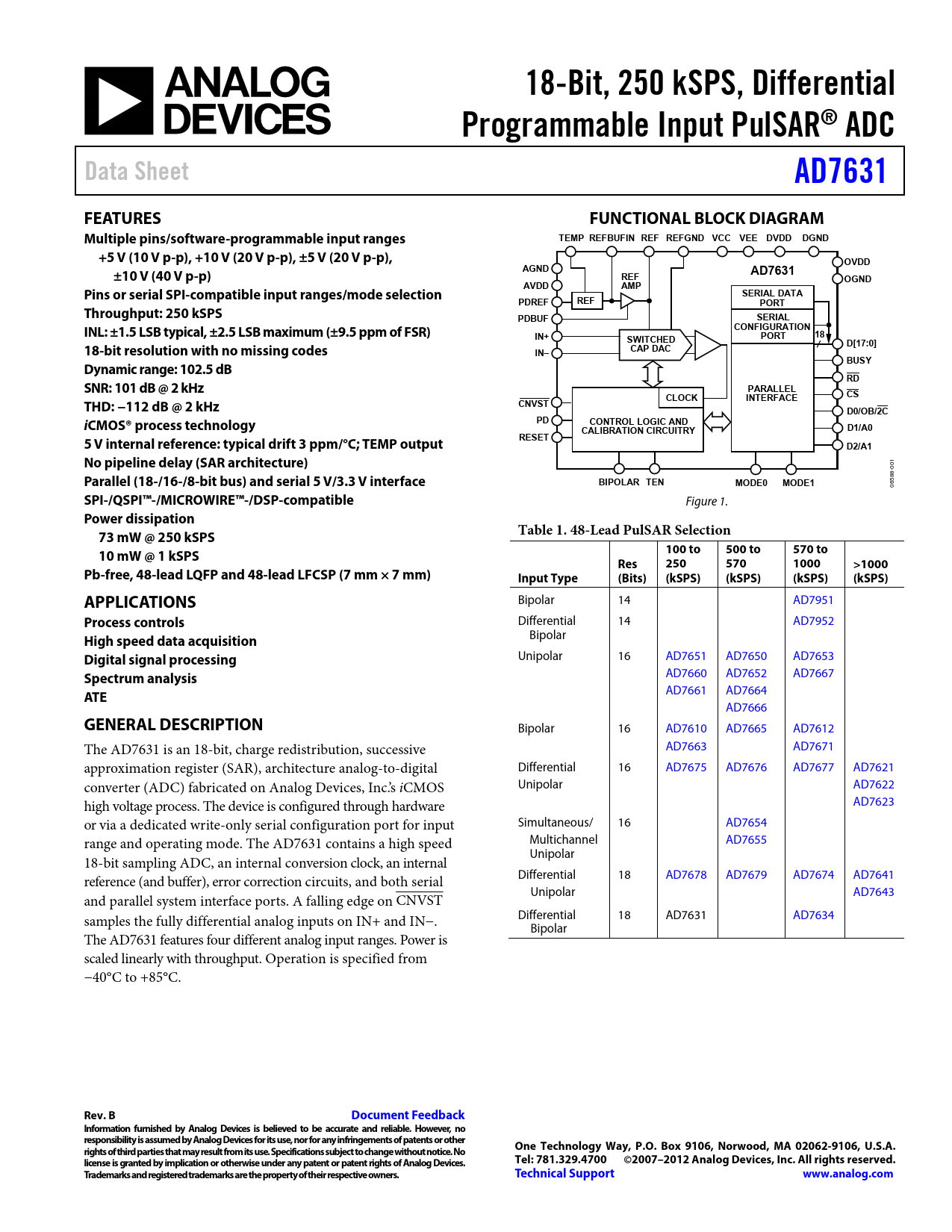
18-Bit, 250 kSPS, Differential. Programmable Input PulSAR® ADC. Data Sheet. AD7631. FEATURES. FUNCTIONAL BLOCK DIAGRAM
Модельный ряд для этого даташита
Текстовая версия документа
18-Bit, 250 kSPS, Differential Programmable Input PulSAR® ADC Data Sheet AD7631 FEATURES FUNCTIONAL BLOCK DIAGRAM Multiple pins/software-programmable input ranges TEMP REFBUFIN REF REFGND VCC VEE DVDD DGND +5 V (10 V p-p), +10 V (20 V p-p), ±5 V (20 V p-p), OVDD AGND ±10 V (40 V p-p) AD7631 REF OGND AVDD AMP Pins or serial SPI-compatible input ranges/mode selection SERIAL DATA PDREF REF PORT Throughput: 250 kSPS PDBUF SERIAL CONFIGURATION INL: ±1.5 LSB typical, ±2.5 LSB maximum (±9.5 ppm of FSR) IN+ PORT 18 SWITCHED D[17:0] 18-bit resolution with no missing codes CAP DAC IN– BUSY Dynamic range: 102.5 dB RD SNR: 101 dB @ 2 kHz PARALLEL CLOCK CS INTERFACE THD: −112 dB @ 2 kHz CNVST D0/OB/2C i CMOS® process technology PD CONTROL LOGIC AND CALIBRATION CIRCUITRY D1/A0 RESET 5 V internal reference: typical drift 3 ppm/°C; TEMP output D2/A1 No pipeline delay (SAR architecture)
1 -00
Parallel (18-/16-/8-bit bus) and serial 5 V/3.3 V interface BIPOLAR TEN MODE0 MODE1
588 06
SPI-/QSPI™-/MICROWIRE™-/DSP-compatible
Figure 1.
Power dissipation Table 1. 48-Lead PulSAR Selection 73 mW @ 250 kSPS 100 to 500 to 570 to 10 mW @ 1 kSPS Res 250 570 1000 >1000 Pb-free, 48-lead LQFP and 48-lead LFCSP (7 mm × 7 mm) Input Type (Bits) (kSPS) (kSPS) (kSPS) (kSPS) APPLICATIONS
Bipolar 14 AD7951
Process controls
Differential 14 AD7952
High speed data acquisition
Bipolar
Digital signal processing
Unipolar 16 AD7651 AD7650 AD7653
Spectrum analysis
AD7660 AD7652 AD7667 AD7661 AD7664
ATE
AD7666
GENERAL DESCRIPTION
Bipolar 16 AD7610 AD7665 AD7612 The AD7631 is an 18-bit, charge redistribution, successive AD7663 AD7671 approximation register (SAR), architecture analog-to-digital Differential 16 AD7675 AD7676 AD7677 AD7621 converter (ADC) fabricated on Analog Devices, Inc.’s iCMOS Unipolar AD7622 high voltage process. The device is configured through hardware AD7623 or via a dedicated write-only serial configuration port for input Simultaneous/ 16 AD7654 range and operating mode. The AD7631 contains a high speed Multichannel AD7655 Unipolar 18-bit sampling ADC, an internal conversion clock, an internal Differential 18 AD7678 AD7679 AD7674 AD7641 reference (and buffer), error correction circuits, and both serial Unipolar AD7643 and parallel system interface ports. A falling edge on CNVST samples the fully differential analog inputs on IN+ and IN−. Differential 18 AD7631 AD7634 Bipolar The AD7631 features four different analog input ranges. Power is scaled linearly with throughput. Operation is specified from −40°C to +85°C.
Rev. B Document Feedback Information furnished by Analog Devices is believed to be accurate and reliable. However, no responsibility is assumed by Analog Devices for its use, nor for any infringements of patents or other One Technology Way, P.O. Box 9106, Norwood, MA 02062-9106, U.S.A. rights of third parties that may result from its use. Specifications subject to change without notice. No license is granted by implication or otherwise under any patent or patent rights of Analog Devices. Tel: 781.329.4700 ©2007–2012 Analog Devices, Inc. All rights reserved. Trademarks and registered trademarks are the property of their respective owners. Technical Support www.analog.com
Document Outline FEATURES APPLICATIONS GENERAL DESCRIPTION FUNCTIONAL BLOCK DIAGRAM TABLE OF CONTENTS REVISION HISTORY SPECIFICATIONS TIMING SPECIFICATIONS ABSOLUTE MAXIMUM RATINGS ESD CAUTION PIN CONFIGURATION AND FUNCTION DESCRIPTIONS TYPICAL PERFORMANCE CHARACTERISTICS TERMINOLOGY THEORY OF OPERATION OVERVIEW CONVERTER OPERATION TRANSFER FUNCTIONS TYPICAL CONNECTION DIAGRAM ANALOG INPUTS Input Range Selection Input Structure Single-to-Differential Driver VOLTAGE REFERENCE INPUT/OUTPUT Internal Reference (REF = 5 V)(PDREF = Low, PDBUF = Low) External 2.5 V Reference and Internal Buffer (REF = 5 V)(PDREF = High, PDBUF = Low) External 5 V Reference (PDREF = High, PDBUF = High) Reference Decoupling Temperature Sensor POWER SUPPLIES Core Supplies High Voltage Supplies Digital Output Supply Power Sequencing Power Dissipation vs. Throughput Power Down CONVERSION CONTROL INTERFACES DIGITAL INTERFACE RESET PARALLEL INTERFACE Master Parallel Interface Slave Parallel Interface 18-Bit Interface (Master or Slave) 16-Bit and 8-Bit Interface (Master or Slave) SERIAL INTERFACE Data Interface Serial Configuration Interface MASTER SERIAL INTERFACE Internal Clock (MODE[1:0] = 3, EXT/ = Low) Read During Convert (RDC = High) Read After Convert (RDC = Low, DIVSCLK[1:0] = [0 to 3]) SLAVE SERIAL INTERFACE External Clock (MODE[1:0] = 3, EXT/ = High) External Discontinuous Clock Data Read After Conversion Daisy-Chain Feature External Clock Data Read During Previous Conversion External Clock Data Read After/During Conversion HARDWARE CONFIGURATION SOFTWARE CONFIGURATION MICROPROCESSOR INTERFACING SPI Interface APPLICATION INFORMATION LAYOUT GUIDELINES EVALUATING PERFORMANCE OUTLINE DIMENSIONS ORDERING GUIDE


