Datasheet AD7622 (Analog Devices)
| Производитель | Analog Devices |
| Описание | 16-Bit, 1.5 LSB INL, 2 MSPS PulSAR® ADC |
| Страниц / Страница | 29 / 1 — 16-Bit, 1.5 LSB INL, 2 MSPS PulSAR® ADC. AD7622. FEATURES. FUNCTIONAL … |
| Формат / Размер файла | PDF / 598 Кб |
| Язык документа | английский |
16-Bit, 1.5 LSB INL, 2 MSPS PulSAR® ADC. AD7622. FEATURES. FUNCTIONAL BLOCK DIAGRAM. Throughput. TEMP REFBUFIN REF REFGND
Модельный ряд для этого даташита
Текстовая версия документа
link to page 4
16-Bit, 1.5 LSB INL, 2 MSPS PulSAR® ADC AD7622 FEATURES FUNCTIONAL BLOCK DIAGRAM Throughput TEMP REFBUFIN REF REFGND DVDD DGND 2 MSPS (wideband warp and warp mode) AGND 1.5 MSPS (normal mode) AD7622 OVDD AVDD INL: ±0.5 LSB typical, ±1.5 LSB maximum (±23 ppm of FSR) OGND REF 16-bit resolution with no missing codes REF AMP SERIAL Dynamic range: 92.5 dB typical PORT IN+ 16 SWITCHED D[15:0] SINAD: 91 dB minimum @ 20 kHz (V CAP DAC REF = 2.5 V) IN– SER/PAR PARALLEL THD: −115 dB typical @ 20 kHz (VREF = 2.5 V) INTERFACE BUSY 2.048 V internal reference: typical drift 8 p pm/°C; TEMP output PDREF CLOCK RD Differential input range: ±VREF (VREF up to 2.5 V) PDBUF CS CONTROL LOGIC AND No pipeline delay (SAR architecture) PD CALIBRATION CIRCUITRY OB/2C Parallel (16-, or 8-bit bus) and serial 5 V/3.3 V/2.5 V interface RESET BYTESWAP
01
SPI®/QSPI™/MICROWIRE™/DSP compatible
0 3- 602 0
Single 2.5 V supply operation WARP NORMAL CNVST Power dissipation
Figure 1.
70 mW typical @ 2 MSPS with internal REF Table 1. PulSAR 48-Lead ADC Selection 2 μW in power-down mode 100 to 500 to 650 to Pb-free, 48-lead LQFP and 48-lead LFCSP_VQ Type/kSPS 250 570 1000 >1000 Pin compatible with other PulSAR 48-lead ADCs
Pseudo AD7651, AD7650, AD7653,
Differential AD7660, AD7652, AD7667 AD7661 AD7664,
APPLICATIONS
AD7666
Medical instruments
True Bipolar AD7610, AD7665 AD7612,
High speed data acquisition/high dynamic data acquisition
AD7663 AD7671
Digital signal processing
True AD7675 AD7676 AD7677 AD7621,
Spectrum analysis
Differential AD7622, AD7623
Instrumentation
18-Bit AD7631, AD7679 AD7634, AD7641,
Communications
Multichannel/ AD7678 AD7674 AD7643
ATE
Simultaneous AD7654 AD7655
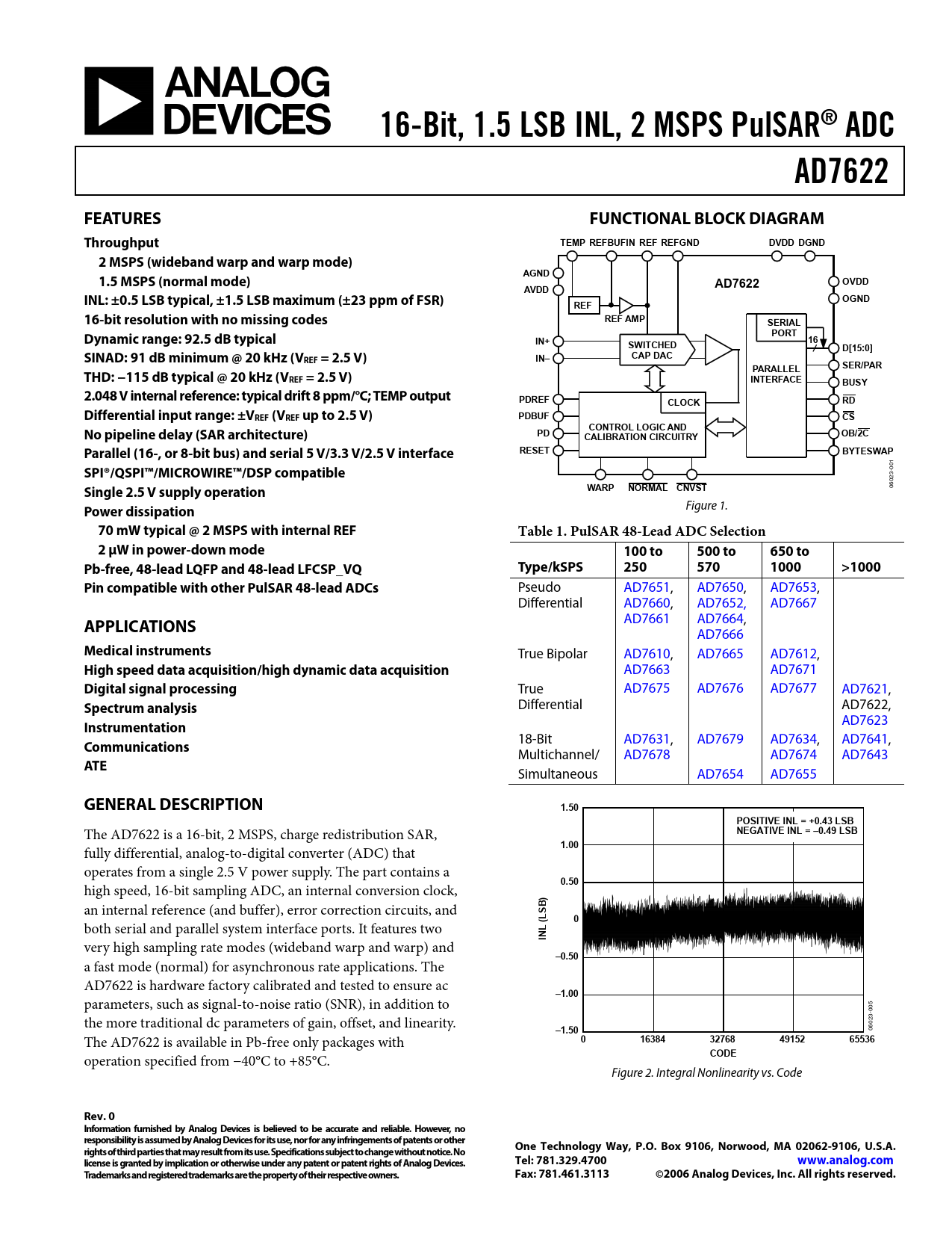
GENERAL DESCRIPTION 1.50 POSITIVE INL = +0.43 LSB
The AD7622 is a 16-bit, 2 MSPS, charge redistribution SAR,
NEGATIVE INL = –0.49 LSB 1.00
fully differential, analog-to-digital converter (ADC) that operates from a single 2.5 V power supply. The part contains a
0.50
high speed, 16-bit sampling ADC, an internal conversion clock,
) B
an internal reference (and buffer), error correction circuits, and
S L 0 (
both serial and parallel system interface ports. It features two
L IN
very high sampling rate modes (wideband warp and warp) and
–0.50
a fast mode (normal) for asynchronous rate applications. The AD7622 is hardware factory calibrated and tested to ensure ac
–1.00
parameters, such as signal-to-noise ratio (SNR), in addition to 05 0 3- the more traditional dc parameters of gain, offset, and linearity. 02
–1.50
06 The AD7622 is available in Pb-free only packages with
0 16384 32768 49152 65536 CODE
operation specified from −40°C to +85°C. Figure 2. Integral Nonlinearity vs. Code
Rev. 0 Information furnished by Analog Devices is believed to be accurate and reliable. However, no responsibility is assumed by Analog Devices for its use, nor for any infringements of patents or other One Technology Way, P.O. Box 9106, Norwood, MA 02062-9106, U.S.A. rights of third parties that may result from its use. Specifications subject to change without notice. No license is granted by implication or otherwise under any patent or patent rights of Analog Devices. Tel: 781.329.4700 www.analog.com Trademarks and registered trademarks are the property of their respective owners. Fax: 781.461.3113 ©2006 Analog Devices, Inc. All rights reserved.
Document Outline FEATURES APPLICATIONS GENERAL DESCRIPTION FUNCTIONAL BLOCK DIAGRAM TABLE OF CONTENTS REVISION HISTORY SPECIFICATIONS ABSOLUTE MAXIMUM RATINGS ESD CAUTION TIMING SPECIFICATIONS PIN CONFIGURATION AND FUNCTION DESCRIPTIONS TERMINOLOGY TYPICAL PERFORMANCE CHARACTERISTICS APPLICATIONS INFORMATION CIRCUIT INFORMATION CONVERTER OPERATION MODES OF OPERATION TRANSFER FUNCTIONS TYPICAL CONNECTION DIAGRAM ANALOG INPUTS MULTIPLEXED INPUTS DRIVER AMPLIFIER CHOICE Single-to-Differential Driver VOLTAGE REFERENCE INPUT Internal Reference (PDBUF = Low, PDREF = Low) External 1.2 V Reference and Internal Buffer (PDBUF = Low, PDREF = High) External 2.5 V Reference (PDBUF = High, PDREF = High) Reference Decoupling Temperature Sensor POWER SUPPLY Power Sequencing Power-Up CONVERSION CONTROL INTERFACES DIGITAL INTERFACE RESET PARALLEL INTERFACE Master Parallel Interface Slave Parallel Interface 8-Bit Interface (Master or Slave) SERIAL INTERFACE MASTER SERIAL INTERFACE Internal Clock SLAVE SERIAL INTERFACE External Clock External Discontinuous Clock Data Read After Conversion External Clock Data Read During Previous Conversion MICROPROCESSOR INTERFACING SPI Interface (ADSP-219x) APPLICATION HINTS LAYOUT EVALUATING THE AD7622 PERFORMANCE OUTLINE DIMENSIONS ORDERING GUIDE

 аккумуляторов")


