Datasheet AD7938, AD7939 (Analog Devices)
| Производитель | Analog Devices |
| Описание | 8-Channel, 1.5 MSPS, 10-Bit Parallel ADCs with a Sequencer |
| Страниц / Страница | 36 / 1 — 8-Channel, 1.5 MSPS, 12-Bit and 10-Bit. Parallel ADCs with a Sequencer. … |
| Версия | E |
| Формат / Размер файла | PDF / 637 Кб |
| Язык документа | английский |
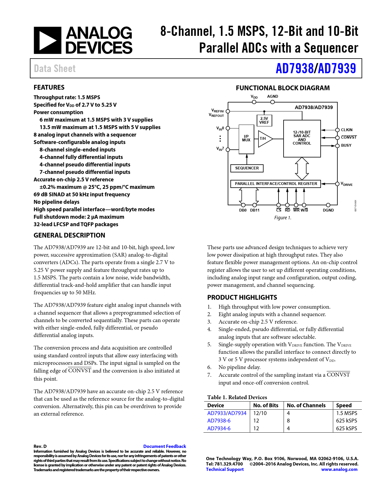
8-Channel, 1.5 MSPS, 12-Bit and 10-Bit. Parallel ADCs with a Sequencer. Data Sheet. AD7938/. AD7939. FEATURES
Модельный ряд для этого даташита
Текстовая версия документа
8-Channel, 1.5 MSPS, 12-Bit and 10-Bit Parallel ADCs with a Sequencer Data Sheet AD7938/ AD7939 FEATURES FUNCTIONAL BLOCK DIAGRAM Throughput rate: 1.5 MSPS VDD AGND Specified for VDD of 2.7 V to 5.25 V AD7938/AD7939 V Power consumption REFIN/ VREFOUT 6 mW maximum at 1.5 MSPS with 3 V supplies 2.5V VREF 13.5 mW maximum at 1.5 MSPS with 5 V supplies VIN0 CLKIN 12-/10-BIT 8 analog input channels with a sequencer I/P SAR ADC T/H CONVST MUX AND Software-configurable analog inputs CONTROL BUSY 8-channel single-ended inputs VIN7 4-channel fully differential inputs 4-channel pseudo differential inputs SEQUENCER 7-channel pseudo differential inputs Accurate on-chip 2.5 V reference PARALLEL INTERFACE/CONTROL REGISTER VDRIVE ±0.2% maximum @ 25°C, 25 ppm/°C maximum 69 dB SINAD at 50 kHz input frequency No pipeline delays
01 0 5-
High speed parallel interface—word/byte modes
71
DB0 DB11 CS RD WR W/B DGND
03
Full shutdown mode: 2 μA maximum
Figure 1.
32-lead LFCSP and TQFP packages GENERAL DESCRIPTION
The AD7938/AD7939 are 12-bit and 10-bit, high speed, low These parts use advanced design techniques to achieve very power, successive approximation (SAR) analog-to-digital low power dissipation at high throughput rates. They also converters (ADCs). The parts operate from a single 2.7 V to feature flexible power management options. An on-chip control 5.25 V power supply and feature throughput rates up to register allows the user to set up different operating conditions, 1.5 MSPS. The parts contain a low noise, wide bandwidth, including analog input range and configuration, output coding, differential track-and-hold amplifier that can handle input power management, and channel sequencing. frequencies up to 50 MHz.
PRODUCT HIGHLIGHTS
The AD7938/AD7939 feature eight analog input channels with 1. High throughput with low power consumption. a channel sequencer that allows a preprogrammed selection of 2. Eight analog inputs with a channel sequencer. channels to be converted sequentially. These parts can operate 3. Accurate on-chip 2.5 V reference. with either single-ended, fully differential, or pseudo 4. Single-ended, pseudo differential, or fully differential differential analog inputs. analog inputs that are software selectable. 5. Single-supply operation with V The conversion process and data acquisition are controlled DRIVE function. The VDRIVE function allows the parallel interface to connect directly to using standard control inputs that allow easy interfacing with 3 V or 5 V processor systems independent of V microprocessors and DSPs. The input signal is sampled on the DD. 6. No pipeline delay. falling edge of CONVST and the conversion is also initiated at 7. Accurate control of the sampling instant via a CONVST this point. input and once-off conversion control. The AD7938/AD7939 have an accurate on-chip 2.5 V reference that can be used as the reference source for the analog-to-digital
Table 1. Related Devices
conversion. Alternatively, this pin can be overdriven to provide
Device No. of Bits No. of Channels Speed
an external reference. AD7933/AD7934 12/10 4 1.5 MSPS AD7938-6 12 8 625 kSPS AD7934-6 12 4 625 kSPS
Rev. D Document Feedback Information furnished by Analog Devices is believed to be accurate and reliable. However, no responsibility is assumed by Analog Devices for its use, nor for any infringements of patents or other rights of third parties that may result from its use. Specifications subject to change without notice. No One Technology Way, P.O. Box 9106, Norwood, MA 02062-9106, U.S.A. license is granted by implication or otherwise under any patent or patent rights of Analog Devices. Tel: 781.329.4700 ©2004–2016 Analog Devices, Inc. All rights reserved. Trademarks and registered trademarks are the property of their respective owners. Technical Support www.analog.com
Document Outline FEATURES GENERAL DESCRIPTION PRODUCT HIGHLIGHTS REVISION HISTORY SPECIFICATIONS AD7938 SPECIFICATIONS AD7939 SPECIFICATIONS TIMING SPECIFICATIONS ABSOLUTE MAXIMUM RATINGS ESD CAUTION PIN CONFIGURATION AND FUNCTION DESCRIPTIONS TYPICAL PERFORMANCE CHARACTERISTICS TERMINOLOGY ON-CHIP REGISTERS CONTROL REGISTER SEQUENCER OPERATION Writing to the Control Register to Program the Sequencer SHADOW REGISTER CIRCUIT INFORMATION CONVERTER OPERATION ADC TRANSFER FUNCTION TYPICAL CONNECTION DIAGRAM ANALOG INPUT STRUCTURE ANALOG INPUTS Single-Ended Mode Differential Mode Driving Differential Inputs Using an Op Amp Pair Pseudo Differential Mode ANALOG INPUT SELECTION Traditional Multichannel Operation (SEQ = SHDW = 0) Using the Sequencer: Programmable Sequence (SEQ = 0, SHDW = 1) Consecutive Sequence (SEQ = 1, SHDW = 1) REFERENCE Digital Inputs VDRIVE Input PARALLEL INTERFACE Reading Data from the AD7938/AD7939 Writing Data to the AD7938/AD7939 POWER MODES OF OPERATION Normal Mode (PM1 = PM0 = 0) Autoshutdown (PM1 = 0; PM0 = 1) Autostandby (PM1 = 1; PM0 = 0) Full Shutdown Mode (PM1 =1; PM0 = 1) POWER vs. THROUGHPUT RATE MICROPROCESSOR INTERFACING AD7938/AD7939 to ADSP-21xx Interface AD7938/AD7939 to ADSP-21065L Interface AD7938/AD7939 to TMS32020, TMS320C25, and TMS320C5x Interface AD7938/AD7939 to 80C186 Interface APPLICATION HINTS GROUNDING AND LAYOUT PCB DESIGN GUIDELINES FOR CHIP SCALE PACKAGE EVALUATING AD7938/AD7939 PERFORMANCE OUTLINE DIMENSIONS ORDERING GUIDE

 аккумуляторов")


