Datasheet AD7441, AD7451 (Analog Devices)
| Производитель | Analog Devices |
| Описание | Pseudo Differential Input, 1 MSPS, 12-Bit ADC in an 8-Lead SOT-23 |
| Страниц / Страница | 24 / 1 — Pseudo Differential Input, 1 MSPS,. 10-/12-Bit ADCs in an 8-Lead SOT-23. … |
| Версия | D |
| Формат / Размер файла | PDF / 523 Кб |
| Язык документа | английский |
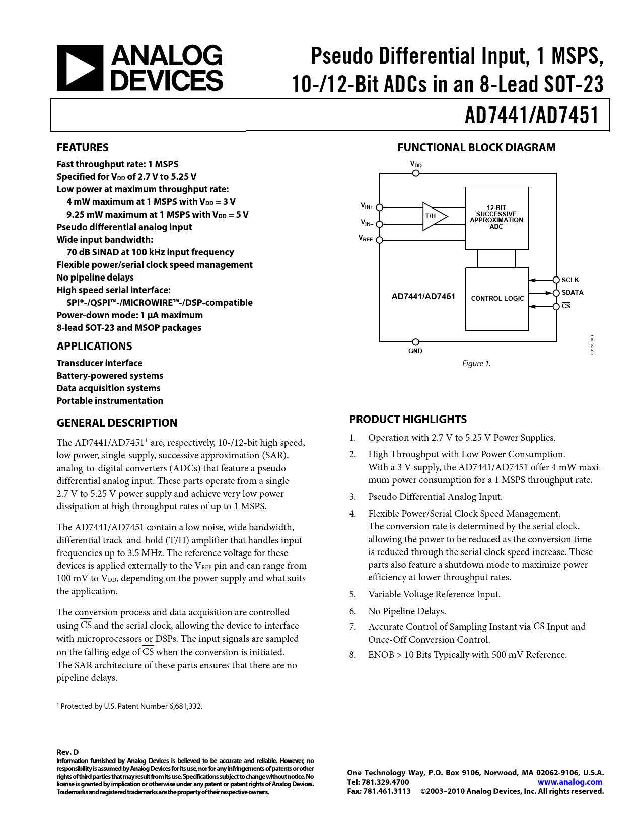
Pseudo Differential Input, 1 MSPS,. 10-/12-Bit ADCs in an 8-Lead SOT-23. AD7441/AD7451. FEATURES. FUNCTIONAL BLOCK DIAGRAM
Модельный ряд для этого даташита
Текстовая версия документа
link to page 1
Pseudo Differential Input, 1 MSPS, 10-/12-Bit ADCs in an 8-Lead SOT-23 AD7441/AD7451 FEATURES FUNCTIONAL BLOCK DIAGRAM Fast throughput rate: 1 MSPS VDD Specified for VDD of 2.7 V to 5.25 V Low power at maximum throughput rate: 4 mW maximum at 1 MSPS with VDD = 3 V VIN+ 12-BIT 9.25 mW maximum at 1 MSPS with V SUCCESSIVE DD = 5 V T/H APPROXIMATION V Pseudo differential analog input IN– ADC Wide input bandwidth: VREF 70 dB SINAD at 100 kHz input frequency Flexible power/serial clock speed management No pipeline delays SCLK High speed serial interface: SDATA AD7441/AD7451 CONTROL LOGIC SPI®-/QSPI™-/MICROWIRE™-/DSP-compatible CS Power-down mode: 1 μA maximum 8-lead SOT-23 and MSOP packages
01 0
APPLICATIONS
3-
GND
15 03
Transducer interface
Figure 1.
Battery-powered systems Data acquisition systems Portable instrumentation GENERAL DESCRIPTION PRODUCT HIGHLIGHTS
1. Operation with 2.7 V to 5.25 V Power Supplies. The AD7441/AD74511 are, respectively, 10-/12-bit high speed, low power, single-supply, successive approximation (SAR), 2. High Throughput with Low Power Consumption. analog-to-digital converters (ADCs) that feature a pseudo With a 3 V supply, the AD7441/AD7451 offer 4 mW maxi- differential analog input. These parts operate from a single mum power consumption for a 1 MSPS throughput rate. 2.7 V to 5.25 V power supply and achieve very low power 3. Pseudo Differential Analog Input. dissipation at high throughput rates of up to 1 MSPS. 4. Flexible Power/Serial Clock Speed Management. The AD7441/AD7451 contain a low noise, wide bandwidth, The conversion rate is determined by the serial clock, differential track-and-hold (T/H) amplifier that handles input allowing the power to be reduced as the conversion time frequencies up to 3.5 MHz. The reference voltage for these is reduced through the serial clock speed increase. These devices is applied externally to the VREF pin and can range from parts also feature a shutdown mode to maximize power 100 mV to VDD, depending on the power supply and what suits efficiency at lower throughput rates. the application. 5. Variable Voltage Reference Input. The conversion process and data acquisition are controlled 6. No Pipeline Delays. using CS and the serial clock, allowing the device to interface 7. Accurate Control of Sampling Instant via CS Input and with microprocessors or DSPs. The input signals are sampled Once-Off Conversion Control. on the falling edge of CS when the conversion is initiated. 8. ENOB > 10 Bits Typically with 500 mV Reference. The SAR architecture of these parts ensures that there are no pipeline delays. 1 Protected by U.S. Patent Number 6,681,332.
Rev. D Information furnished by Analog Devices is believed to be accurate and reliable. However, no responsibility is assumed by Analog Devices for its use, nor for any infringements of patents or other One Technology Way, P.O. Box 9106, Norwood, MA 02062-9106, U.S.A. rights of third parties that may result from its use. Specifications subject to change without notice. No license is granted by implication or otherwise under any patent or patent rights of Analog Devices. Tel: 781.329.4700 www.analog.com Trademarks and registered trademarks are the property of their respective owners. Fax: 781.461.3113 ©2003–2010 Analog Devices, Inc. All rights reserved.
Document Outline FEATURES APPLICATIONS FUNCTIONAL BLOCK DIAGRAM GENERAL DESCRIPTION PRODUCT HIGHLIGHTS TABLE OF CONTENTS REVISION HISTORY SPECIFICATIONS TIMING SPECIFICATIONS TIMING DIAGRAMS ABSOLUTE MAXIMUM RATINGS ESD CAUTION PIN CONFIGURATIONS AND FUNCTION DESCRIPTIONS TYPICAL PERFORMANCE CHARACTERISTICS TERMINOLOGY THEORY OF OPERATION CIRCUIT INFORMATION CONVERTER OPERATION ADC TRANSFER FUNCTION TYPICAL CONNECTION DIAGRAM ANALOG INPUT ANALOG INPUT STRUCTURE DIGITAL INPUTS REFERENCE SERIAL INTERFACE Timing Example 1 Timing Example 2 MODES OF OPERATION NORMAL MODE POWER-DOWN MODE Power-Up Time POWER VS. THROUGHPUT RATE MICROPROCESSOR AND DSP INTERFACING AD7441/AD7451 to ADSP-21xx AD7441/AD7451 to TMS320C5x/C54x AD7441/AD7451 to DSP56xxx GROUNDING AND LAYOUT HINTS EVALUATING PERFORMANCE OUTLINE DIMENSIONS ORDERING GUIDE

 аккумуляторов")


