Datasheet AD7466, AD7467, AD7468 (Analog Devices)
| Производитель | Analog Devices |
| Описание | 1.6 V Micro-Power 8-Bit ADC |
| Страниц / Страница | 28 / 1 — 1.6 V, Micropower 12-/10-/8-Bit ADCs. AD7466/AD7467/AD7468. FEATURES. … |
| Версия | C |
| Формат / Размер файла | PDF / 460 Кб |
| Язык документа | английский |
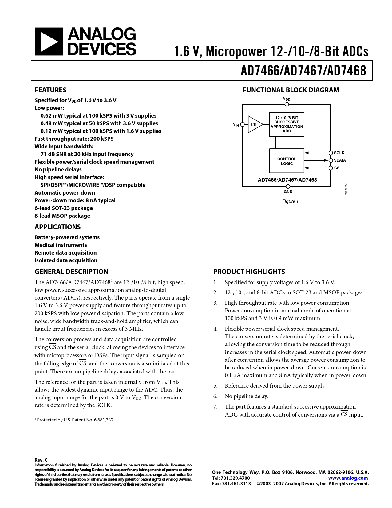
1.6 V, Micropower 12-/10-/8-Bit ADCs. AD7466/AD7467/AD7468. FEATURES. FUNCTIONAL BLOCK DIAGRAM. Specified for V. VDD
Модельный ряд для этого даташита
Текстовая версия документа
link to page 1
1.6 V, Micropower 12-/10-/8-Bit ADCs AD7466/AD7467/AD7468 FEATURES FUNCTIONAL BLOCK DIAGRAM Specified for V VDD DD of 1.6 V to 3.6 V Low power: 0.62 mW typical at 100 kSPS with 3 V supplies 12-/10-/8-BIT 0.48 mW typical at 50 kSPS with 3.6 V supplies SUCCESSIVE VIN T/H APPROXIMATION 0.12 mW typical at 100 kSPS with 1.6 V supplies ADC Fast throughput rate: 200 kSPS Wide input bandwidth: 71 dB SNR at 30 kHz input frequency SCLK CONTROL Flexible power/serial clock speed management SDATA LOGIC No pipeline delays CS High speed serial interface: AD7466/AD7467/AD7468 SPI/QSPI™/MICROWIRE™/DSP compatible Automatic power-down GND
02643-001
Power-down mode: 8 nA typical
Figure 1.
6-lead SOT-23 package 8-lead MSOP package APPLICATIONS Battery-powered systems Medical instruments Remote data acquisition Isolated data acquisition GENERAL DESCRIPTION PRODUCT HIGHLIGHTS
The AD7466/AD7467/AD74681 are 12-/10-/8-bit, high speed, 1. Specified for supply voltages of 1.6 V to 3.6 V. low power, successive approximation analog-to-digital 2. 12-, 10-, and 8-bit ADCs in SOT-23 and MSOP packages. converters (ADCs), respectively. The parts operate from a single 1.6 V to 3.6 V power supply and feature throughput rates up to 3. High throughput rate with low power consumption. 200 kSPS with low power dissipation. The parts contain a low Power consumption in normal mode of operation at noise, wide bandwidth track-and-hold amplifier, which can 100 kSPS and 3 V is 0.9 mW maximum. handle input frequencies in excess of 3 MHz. 4. Flexible power/serial clock speed management. The conversion process and data acquisition are controlled The conversion rate is determined by the serial clock, allowing the conversion time to be reduced through using CS and the serial clock, allowing the devices to interface increases in the serial clock speed. Automatic power-down with microprocessors or DSPs. The input signal is sampled on after conversion allows the average power consumption to the falling edge of CS, and the conversion is also initiated at this be reduced when in power-down. Current consumption is point. There are no pipeline delays associated with the part. 0.1 μA maximum and 8 nA typically when in power-down. The reference for the part is taken internally from VDD. This 5. Reference derived from the power supply. allows the widest dynamic input range to the ADC. Thus, the analog input range for the part is 0 V to V 6. No pipeline delay. DD. The conversion rate is determined by the SCLK. 7. The part features a standard successive approximation ADC with accurate control of conversions via a CS input. 1 Protected by U.S. Patent No. 6,681,332.
Rev. C Information furnished by Analog Devices is believed to be accurate and reliable. However, no responsibility is assumed by Analog Devices for its use, nor for any infringements of patents or other One Technology Way, P.O. Box 9106, Norwood, MA 02062-9106, U.S.A. rights of third parties that may result from its use. Specifications subject to change without notice. No license is granted by implication or otherwise under any patent or patent rights of Analog Devices. Tel: 781.329.4700 www.analog.com Trademarks and registered trademarks are the property of their respective owners. Fax: 781.461.3113 ©2003–2007 Analog Devices, Inc. All rights reserved.
Document Outline FEATURES APPLICATIONS FUNCTIONAL BLOCK DIAGRAM GENERAL DESCRIPTION PRODUCT HIGHLIGHTS TABLE OF CONTENTS REVISION HISTORY SPECIFICATIONS AD7466 AD7467 AD7468 TIMING SPECIFICATIONS TIMING EXAMPLES Timing Example 1 Timing Example 2 ABSOLUTE MAXIMUM RATINGS ESD CAUTION PIN CONFIGURATIONS AND FUNCTION DESCRIPTIONS TYPICAL PERFORMANCE CHARACTERISTICS DYNAMIC PERFORMANCE CURVES DC ACCURACY CURVES POWER REQUIREMENT CURVES TERMINOLOGY THEORY OF OPERATION CIRCUIT INFORMATION CONVERTER OPERATION ADC TRANSFER FUNCTION TYPICAL CONNECTION DIAGRAM ANALOG INPUT DIGITAL INPUTS NORMAL MODE POWER CONSUMPTION Power Consumption Example 1 Power Consumption Example 2 SERIAL INTERFACE MICROPROCESSOR INTERFACING AD7466/AD7467/AD7468 to TMS320C541 Interface AD7466/AD7467/AD7468 to ADSP-218x Interface AD7466/AD7467/AD7468 to DSP563xx Interface APPLICATION HINTS GROUNDING AND LAYOUT EVALUATING THE PERFORMANCE OF THE AD7466 AND AD7467 OUTLINE DIMENSIONS ORDERING GUIDE

 аккумуляторов")


