Datasheet AD9203 (Analog Devices)
| Производитель | Analog Devices |
| Описание | 10-Bit, 40 MSPS, Low-Power Analog-to-Digital Converter |
| Страниц / Страница | 29 / 1 — 10-Bit, 40 MSPS, 3 V, 74 mW. A/D Converter. AD9203. FEATURES. FUNCTIONAL … |
| Версия | B |
| Формат / Размер файла | PDF / 1.1 Мб |
| Язык документа | английский |
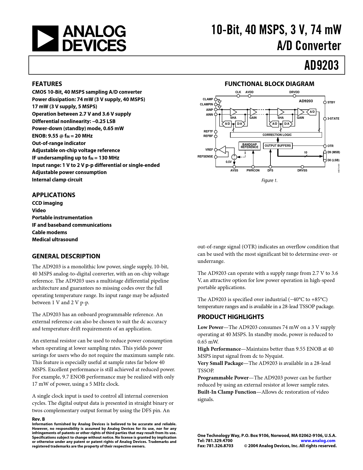
10-Bit, 40 MSPS, 3 V, 74 mW. A/D Converter. AD9203. FEATURES. FUNCTIONAL BLOCK DIAGRAM
Модельный ряд для этого даташита
Текстовая версия документа
10-Bit, 40 MSPS, 3 V, 74 mW A/D Converter AD9203 FEATURES FUNCTIONAL BLOCK DIAGRAM CMOS 10-Bit, 40 MSPS sampling A/D converter CLK AVDD DRVDD Power dissipation: 74 mW (3 V supply, 40 MSPS) CLAMP AD9203 STBY 17 mW (3 V supply, 5 MSPS) CLAMPIN AINP Operation between 2.7 V and 3.6 V supply A/D AINN SHA GAIN SHA GAIN 3-STATE Differential nonlinearity: −0.25 LSB A/D D/A A/D D/A Power-down (standby) mode, 0.65 mW REFTF ENOB: 9.55 @ f CORRECTION LOGIC IN = 20 MHz REFBF Out-of-range indicator BANDGAP OUTPUT BUFFERS OTR REFERENCE Adjustable on-chip voltage reference VREF 10 D9 (MSB) + IF undersampling up to f REFSENSE IN = 130 MHz – D0 (LSB) 0.5V Input range: 1 V to 2 V p-p differential or single-ended Adjustable power consumption AVSS PWRCON DFS DRVSS
00573-001
Internal clamp circuit
Figure 1.
APPLICATIONS CCD imaging Video Portable instrumentation IF and baseband communications Cable modems Medical ultrasound
out-of-range signal (OTR) indicates an overflow condition that
GENERAL DESCRIPTION
can be used with the most significant bit to determine over- or underrange. The AD9203 is a monolithic low power, single supply, 10-bit, 40 MSPS analog-to-digital converter, with an on-chip voltage The AD9203 can operate with a supply range from 2.7 V to 3.6 reference. The AD9203 uses a multistage differential pipeline V, an attractive option for low power operation in high-speed architecture and guarantees no missing codes over the full portable applications. operating temperature range. Its input range may be adjusted The AD9203 is specified over industrial (−40°C to +85°C) between 1 V and 2 V p-p. temperature ranges and is available in a 28-lead TSSOP package. The AD9203 has an onboard programmable reference. An
PRODUCT HIGHLIGHTS
external reference can also be chosen to suit the dc accuracy and temperature drift requirements of an application.
Low Power
—The AD9203 consumes 74 mW on a 3 V supply operating at 40 MSPS. In standby mode, power is reduced to An external resistor can be used to reduce power consumption 0.65 mW. when operating at lower sampling rates. This yields power
High Performance
—Maintains better than 9.55 ENOB at 40 savings for users who do not require the maximum sample rate. MSPS input signal from dc to Nyquist. This feature is especially useful at sample rates far below 40
Very Small Package
—The AD9203 is available in a 28-lead MSPS. Excellent performance is still achieved at reduced power. TSSOP. For example, 9.7 ENOB performance may be realized with only
Programmable Power
—The AD9203 power can be further 17 mW of power, using a 5 MHz clock. reduced by using an external resistor at lower sample rates.
Built-In Clamp Function
—Allows dc restoration of video A single clock input is used to control all internal conversion signals. cycles. The digital output data is presented in straight binary or twos complementary output format by using the DFS pin. An
Rev. B Information furnished by Analog Devices is believed to be accurate and reliable. However, no responsibility is assumed by Analog Devices for its use, nor for any infringements of patents or other rights of third parties that may result from its use. Specifications subject to change without notice. No license is granted by implication One Technology Way, P.O. Box 9106, Norwood, MA 02062-9106, U.S.A. or otherwise under any patent or patent rights of Analog Devices. Trademarks and Tel: 781.329.4700 www.analog.com registered trademarks are the property of their respective owners. Fax: 781.326.8703 © 2004 Analog Devices, Inc. All rights reserved.
Document Outline FEATURES GENERAL DESCRIPTION FUNCTIONAL BLOCK DIAGRAM PRODUCT HIGHLIGHTS SPECIFICATIONS ABSOLUTE MAXIMUM RATINGS THERMAL CHARACTERISTICS ESD CAUTION PIN CONFIGURATION AND FUNCTION DESCRIPTIONS TERMINOLOGY TYPICAL PERFORMANCE CHARACTERISTICS OPERATIONS THEORY OF OPERATION OPERATIONAL MODES INPUT AND REFERENCE OVERVIEW INTERNAL REFERENCE CONNECTION EXTERNAL REFERENCE OPERATION CLAMP OPERATION DRIVING THE ANALOG INPUT OP AMP SELECTION GUIDE DIFFERENTIAL MODE OF OPERATION POWER CONTROL INTERFACING TO 5 V SYSTEMS CLOCK INPUT AND CONSIDERATIONS DIGITAL INPUTS AND OUTPUTS APPLICATIONS DIRECT IF DOWN CONVERSION ULTRASOUND APPLICATIONS EVALUATION BOARD OUTLINE DIMENSIONS ORDERING GUIDE

 аккумуляторов")


