Datasheet AD7707 (Analog Devices)
| Производитель | Analog Devices |
| Описание | 3 V/5 V, ±10 V Input Range, 1 mW 3-Channel 16-Bit, Sigma-Delta ADC |
| Страниц / Страница | 53 / 1 — 3 V/5 V, ±10 V Input Range, 1 mW. 3-Channel 16-Bit, Sigma-Delta ADC. … |
| Версия | B |
| Формат / Размер файла | PDF / 788 Кб |
| Язык документа | английский |
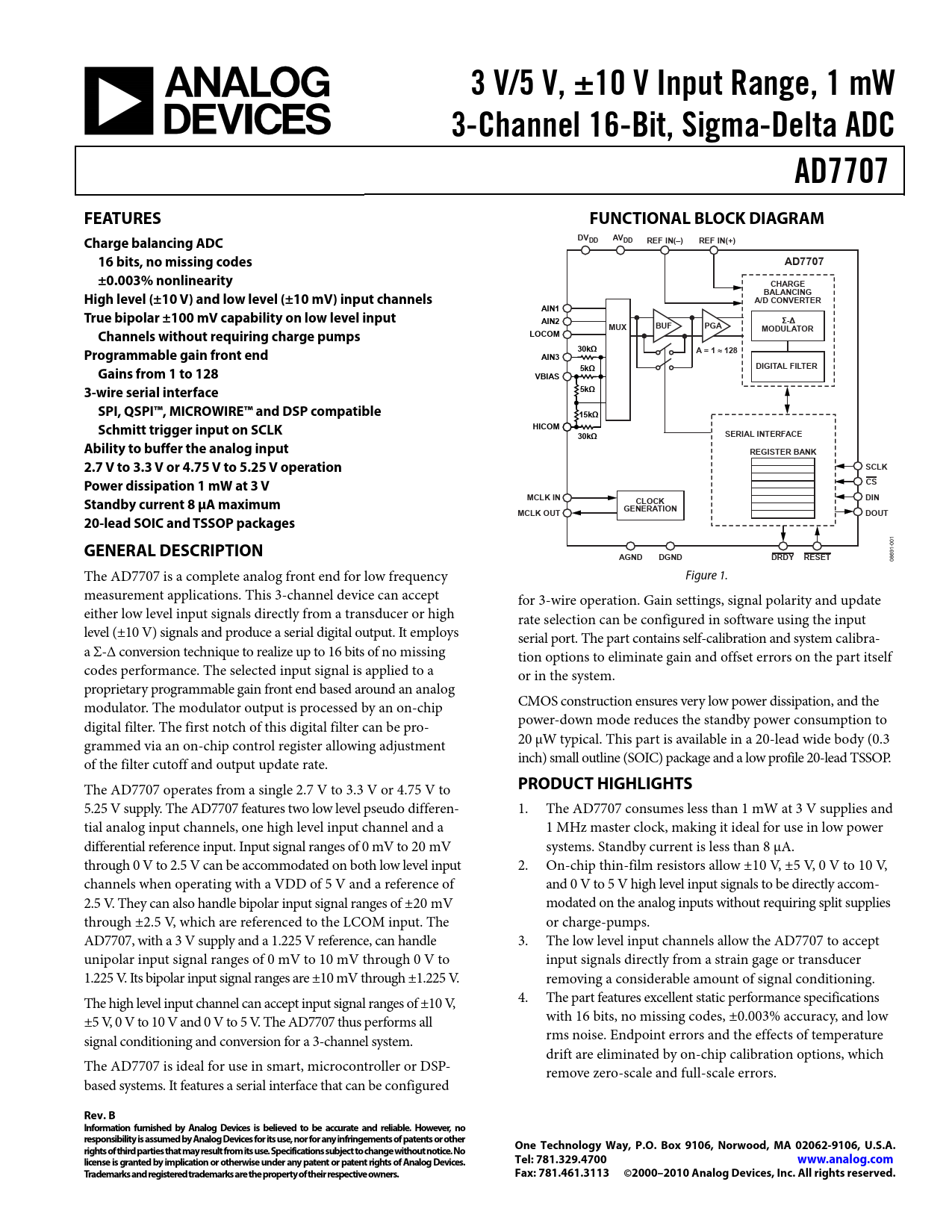
3 V/5 V, ±10 V Input Range, 1 mW. 3-Channel 16-Bit, Sigma-Delta ADC. AD7707. FEATURES. FUNCTIONAL BLOCK DIAGRAM
Модельный ряд для этого даташита
Текстовая версия документа
3 V/5 V, ±10 V Input Range, 1 mW 3-Channel 16-Bit, Sigma-Delta ADC AD7707 FEATURES FUNCTIONAL BLOCK DIAGRAM DV Charge balancing ADC DD AVDD REF IN(–) REF IN(+) 16 bits, no missing codes AD7707 ±0.003% nonlinearity CHARGE BALANCING High level (±10 V) and low level (±10 mV) input channels A/D CONVERTER AIN1 True bipolar ±100 mV capability on low level input AIN2 Σ-Δ MUX BUF PGA MODULATOR Channels without requiring charge pumps LOCOM 30kΩ Programmable gain front end A = 1 ≈ 128 AIN3 DIGITAL FILTER 5kΩ Gains from 1 to 128 VBIAS 3-wire serial interface 5kΩ SPI, QSPI™, MICROWIRE™ and DSP compatible 15kΩ Schmitt trigger input on SCLK HICOM SERIAL INTERFACE 30kΩ Ability to buffer the analog input REGISTER BANK 2.7 V to 3.3 V or 4.75 V to 5.25 V operation SCLK Power dissipation 1 mW at 3 V CS MCLK IN DIN Standby current 8 μA maximum CLOCK GENERATION MCLK OUT DOUT 20-lead SOIC and TSSOP packages
1
GENERAL DESCRIPTION
-00 91
AGND DGND DRDY RESET
086 The AD7707 is a complete analog front end for low frequency Figure 1. measurement applications. This 3-channel device can accept for 3-wire operation. Gain settings, signal polarity and update either low level input signals directly from a transducer or high rate selection can be configured in software using the input level (±10 V) signals and produce a serial digital output. It employs serial port. The part contains self-calibration and system calibra- a Σ-Δ conversion technique to realize up to 16 bits of no missing tion options to eliminate gain and offset errors on the part itself codes performance. The selected input signal is applied to a or in the system. proprietary programmable gain front end based around an analog modulator. The modulator output is processed by an on-chip CMOS construction ensures very low power dissipation, and the digital filter. The first notch of this digital filter can be pro- power-down mode reduces the standby power consumption to grammed via an on-chip control register allowing adjustment 20 μW typical. This part is available in a 20-lead wide body (0.3 of the filter cutoff and output update rate. inch) small outline (SOIC) package and a low profile 20-lead TSSOP. The AD7707 operates from a single 2.7 V to 3.3 V or 4.75 V to
PRODUCT HIGHLIGHTS
5.25 V supply. The AD7707 features two low level pseudo differen- 1. The AD7707 consumes less than 1 mW at 3 V supplies and tial analog input channels, one high level input channel and a 1 MHz master clock, making it ideal for use in low power differential reference input. Input signal ranges of 0 mV to 20 mV systems. Standby current is less than 8 μA. through 0 V to 2.5 V can be accommodated on both low level input 2. On-chip thin-film resistors allow ±10 V, ±5 V, 0 V to 10 V, channels when operating with a VDD of 5 V and a reference of and 0 V to 5 V high level input signals to be directly accom- 2.5 V. They can also handle bipolar input signal ranges of ±20 mV modated on the analog inputs without requiring split supplies through ±2.5 V, which are referenced to the LCOM input. The or charge-pumps. AD7707, with a 3 V supply and a 1.225 V reference, can handle 3. The low level input channels allow the AD7707 to accept unipolar input signal ranges of 0 mV to 10 mV through 0 V to input signals directly from a strain gage or transducer 1.225 V. Its bipolar input signal ranges are ±10 mV through ±1.225 V. removing a considerable amount of signal conditioning. The high level input channel can accept input signal ranges of ±10 V, 4. The part features excellent static performance specifications ±5 V, 0 V to 10 V and 0 V to 5 V. The AD7707 thus performs all with 16 bits, no missing codes, ±0.003% accuracy, and low signal conditioning and conversion for a 3-channel system. rms noise. Endpoint errors and the effects of temperature drift are eliminated by on-chip calibration options, which The AD7707 is ideal for use in smart, microcontroller or DSP- remove zero-scale and full-scale errors. based systems. It features a serial interface that can be configured
Rev. B Information furnished by Analog Devices is believed to be accurate and reliable. However, no responsibility is assumed by Analog Devices for its use, nor for any infringements of patents or other One Technology Way, P.O. Box 9106, Norwood, MA 02062-9106, U.S.A. rights of third parties that may result from its use. Specifications subject to change without notice. No license is granted by implication or otherwise under any patent or patent rights of Analog Devices. Tel: 781.329.4700 www.analog.com Trademarks and registered trademarks are the property of their respective owners. Fax: 781.461.3113 ©2000–2010 Analog Devices, Inc. All rights reserved.
Document Outline FEATURES GENERAL DESCRIPTION FUNCTIONAL BLOCK DIAGRAM PRODUCT HIGHLIGHTS TABLE OF CONTENTS REVISION HISTORY SPECIFICATIONS TIMING CHARACTERISTICS ABSOLUTE MAXIMUM RATINGS ESD CAUTION PIN CONFIGURATION AND FUNCTION DESCRIPTIONS TYPICAL PERFORMANCE CHARACTERISTICS OUTPUT NOISE OUTPUT NOISE FOR LOW LEVEL INPUT CHANNELS (5 V OPERATION) OUTPUT NOISE FOR LOW LEVEL INPUT CHANNELS (3 V OPERATION) OUTPUT NOISE FOR HIGH LEVEL INPUT CHANNEL AIN3 (5 V OPERATION) OUTPUT NOISE FOR HIGH LEVEL INPUT CHANNEL AIN3 (3 V OPERATION) ON-CHIP REGISTERS COMMUNICATIONS REGISTER (RS2, RS1, RS0 = 0, 0, 0) Setup Register (RS2, RS1, RS0 = 0, 0, 1); Power-On/Reset Status: 0x01 Clock Register (RS2, RS1, RS0 = 0, 1, 0); Power-On/Reset Status: 0x05 Data Register (RS2, RS1, RS0 = 0, 1, 1) Test Register (RS2, RS1, RS0 = 1, 0, 0); Power-On/Reset Status: 0x00 Zero-Scale Calibration Register (RS2, RS1, RS0 = 1, 1, 0); Power-On/Reset Status: 0x1F4000 Full-Scale Calibration Register (RS2, RS1, RS0 = 1, 1, 1); Power-On/Reset Status: 0x5761AB CALIBRATION SEQUENCES CIRCUIT DESCRIPTION ANALOG INPUT ANALOG INPUT RANGES INPUT SAMPLE RATE BIPOLAR/UNIPOLAR INPUTS REFERENCE INPUT DIGITAL FILTERING FILTER CHARACTERISTICS POSTFILTERING ANALOG FILTERING CALIBRATION SELF-CALIBRATION SYSTEM CALIBRATION SPAN AND OFFSET LIMITS ON THE LOW LEVEL INPUT CHANNELS, AIN1 AND AIN2 SPAN AND OFFSET LIMITS ON THE HIGH LEVEL INPUT CHANNEL AIN3 POWER-UP AND CALIBRATION USING THE AD7707 CLOCKING AND OSCILLATOR CIRCUIT SYSTEM SYNCHRONIZATION RESET INPUT STANDBY MODE ACCURACY DRIFT CONSIDERATIONS POWER SUPPLIES SUPPLY CURRENT GROUNDING AND LAYOUT DIGITAL INTERFACE CONFIGURING THE AD7707 MICROCOMPUTER/MICROPROCESSOR INTERFACING AD7707 TO 68HC11 INTERFACE AD7707 TO 8XC51 INTERFACE CODE FOR SETTING UP THE AD7707 C CODE FOR INTERFACING AD7707 TO 68HC11 APPLICATIONS INFORMATION DATA ACQUISITION SMART VALVE/ACTUATOR CONTROL PRESSURE MEASUREMENT THERMOCOUPLE MEASUREMENT RTD MEASUREMENT CHART RECORDERS ACCOMMODATING VARIOUS HIGH LEVEL INPUT RANGES TYPICAL INPUT CURRENTS OUTPUT NOISE FOR HIGH LEVEL INPUT CHANNEL, AIN3 5 V OPERATION 3 V OPERATION OUTLINE DIMENSIONS ORDERING GUIDE

 аккумуляторов")


