Datasheet AD7817, AD7818 (Analog Devices)
| Производитель | Analog Devices |
| Описание | Temperature Sensor (On Chip) 4-Channel, 9 µs, 10-Bit ADC |
| Страниц / Страница | 20 / 1 — 4-Channel/Single-Channel, 9 μs,. 10-Bit ADCs with On-Chip Temperature … |
| Версия | E |
| Формат / Размер файла | PDF / 351 Кб |
| Язык документа | английский |
4-Channel/Single-Channel, 9 μs,. 10-Bit ADCs with On-Chip Temperature Sensor. Data Sheet. AD7817. /AD7818. FEATURES
Модельный ряд для этого даташита
Текстовая версия документа
link to page 14 link to page 17 link to page 17 link to page 18 link to page 18
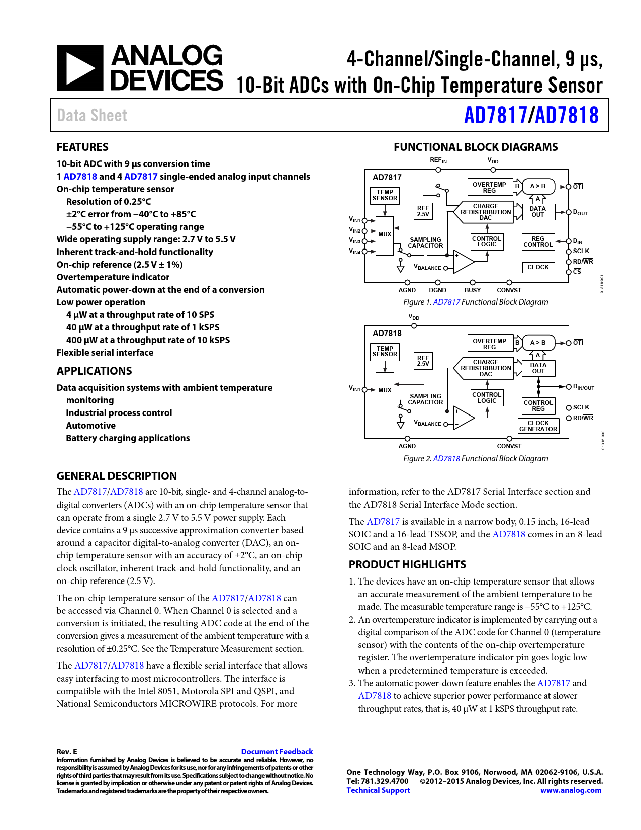
4-Channel/Single-Channel, 9 μs, 10-Bit ADCs with On-Chip Temperature Sensor Data Sheet AD7817 /AD7818 FEATURES FUNCTIONAL BLOCK DIAGRAMS REF V 10-bit ADC with 9 μs conversion time IN DD 1 AD7818 and 4 AD7817 singl e-ended analog input channels AD7817 OVERTEMP On-chip temperature sensor B A > B OTI TEMP REG SENSOR Resolution of 0.25°C A REF CHARGE DATA ±2°C error from −40°C to +85°C 2.5V REDISTRIBUTION DOUT OUT V DAC IN1 −55°C to +125°C operating range VIN2 MUX Wide operating supply range: 2.7 V to 5.5 V V CONTROL REG IN3 SAMPLING D CAPACITOR IN LOGIC CONTROL Inherent track-and-hold functionality VIN4 SCLK On-chip reference (2.5 V ± 1%) RD/WR VBALANCE CLOCK CS Overtemperature indicator
1 00 6-
Automatic power-down at the end of a conversion AGND DGND BUSY CONVST
131 0
Low power operation
Figure 1. AD7817 Functional Block Diagram
4 μW at a throughput rate of 10 SPS VDD 40 μW at a throughput rate of 1 kSPS AD7818 400 μW at a throughput rate of 10 kSPS OVERTEMP B A > B OTI TEMP REG Flexible serial interface SENSOR REF A 2.5V CHARGE DATA APPLICATIONS REDISTRIBUTION OUT DAC Data acquisition systems with ambient temperature V D IN1 MUX IN/OUT SAMPLING CONTROL monitoring CAPACITOR LOGIC CONTROL SCLK REG Industrial process control RD/WR Automotive VBALANCE CLOCK GENERATOR
2
Battery charging applications
00 6-
AGND CONVST
131 0 Figure 2. AD7818 Functional Block Diagram
GENERAL DESCRIPTION
The AD7817/AD7818 are 10-bit, single- and 4-channel analog-to- information, refer to the AD7817 Serial Interface section and digital converters (ADCs) with an on-chip temperature sensor that the AD7818 Serial Interface Mode section. can operate from a single 2.7 V to 5.5 V power supply. Each The AD7817 is available in a narrow body, 0.15 inch, 16-lead device contains a 9 μs successive approximation converter based SOIC and a 16-lead TSSOP, and the AD7818 comes in an 8-lead around a capacitor digital-to-analog converter (DAC), an on- SOIC and an 8-lead MSOP. chip temperature sensor with an accuracy of ±2°C, an on-chip clock oscillator, inherent track-and-hold functionality, and an
PRODUCT HIGHLIGHTS
on-chip reference (2.5 V). 1. The devices have an on-chip temperature sensor that allows The on-chip temperature sensor of the AD7817/AD7818 can an accurate measurement of the ambient temperature to be be accessed via Channel 0. When Channel 0 is selected and a made. The measurable temperature range is −55°C to +125°C. conversion is initiated, the resulting ADC code at the end of the 2. An overtemperature indicator is implemented by carrying out a conversion gives a measurement of the ambient temperature with a digital comparison of the ADC code for Channel 0 (temperature resolution of ±0.25°C. See the Temperature Measurement section. sensor) with the contents of the on-chip overtemperature register. The overtemperature indicator pin goes logic low The AD7817/AD7818 have a flexible serial interface that allows when a predetermined temperature is exceeded. easy interfacing to most microcontrollers. The interface is 3. The automatic power-down feature enables the AD7817 and compatible with the Intel 8051, Motorola SPI and QSPI, and AD7818 to achieve superior power performance at slower National Semiconductors MICROWIRE protocols. For more throughput rates, that is, 40 μW at 1 kSPS throughput rate.
Rev. E Document Feedback Information furnished by Analog Devices is believed to be accurate and reliable. However, no responsibility is assumed by Analog Devices for its use, nor for any infringements of patents or other rights of third parties that may result from its use. Specifications subject to change without notice. No One Technology Way, P.O. Box 9106, Norwood, MA 02062-9106, U.S.A. license is granted by implication or otherwise under any patent or patent rights of Analog Devices. Tel: 781.329.4700 ©2012–2015 Analog Devices, Inc. All rights reserved. Trademarks and registered trademarks are the property of their respective owners. Technical Support www.analog.com
Document Outline FEATURES APPLICATIONS FUNCTIONAL BLOCK DIAGRAMS GENERAL DESCRIPTION PRODUCT HIGHLIGHTS TABLE OF CONTENTS REVISION HISTORY SPECIFICATIONS TIMING CHARACTERISTICS ABSOLUTE MAXIMUM RATINGS ESD CAUTION PIN CONFIGURATIONS AND FUNCTION DESCRIPTIONS TERMINOLOGY CONTROL BYTE Address Register Overtemperature Register CIRCUIT INFORMATION CONVERTER DETAILS TYPICAL CONNECTION DIAGRAM ANALOG INPUTS Analog Input DC Acquisition Time AC Acquisition Time ON-CHIP REFERENCE ADC TRANSFER FUNCTION TEMPERATURE MEASUREMENT TEMPERATURE MEASUREMENT ERROR DUE TO REFERENCE ERROR SELF-HEATING CONSIDERATIONS OPERATING MODES Mode 1 Mode 2 POWER vs. THROUGHPUT AD7817 SERIAL INTERFACE Read Operation Write Operation Simplifying the Serial Interface AD7818 SERIAL INTERFACE MODE Read Operation Write Operation OUTLINE DIMENSIONS ORDERING GUIDE

 аккумуляторов")


