Datasheet AD7712 (Analog Devices)
| Производитель | Analog Devices |
| Описание | CMOS, 24-Bit Sigma-Delta, Signal Conditioning ADC with 2 Analog Input Channels |
| Страниц / Страница | 29 / 1 — LC2MOS. Signal Conditioning ADC. AD7712. FEATURES. FUNCTIONAL BLOCK … |
| Версия | F |
| Формат / Размер файла | PDF / 306 Кб |
| Язык документа | английский |
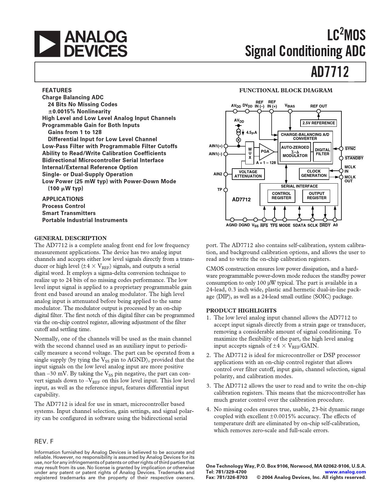
LC2MOS. Signal Conditioning ADC. AD7712. FEATURES. FUNCTIONAL BLOCK DIAGRAM. Charge Balancing ADC. REF. 24 Bits No Missing Codes
Модельный ряд для этого даташита
Текстовая версия документа
LC2MOS Signal Conditioning ADC AD7712 FEATURES FUNCTIONAL BLOCK DIAGRAM Charge Balancing ADC REF REF 24 Bits No Missing Codes AV DV DD DD IN (–) IN (+) VBIAS REF OUT
ⴞ
0.0015% Nonlinearity High Level and Low Level Analog Input Channels AVDD 2.5V REFERENCE Programmable Gain for Both Inputs Gains from 1 to 128 4.5
A CHARGE-BALANCING A/D CONVERTER Differential Input for Low Level Channel AIN1(+) Low-Pass Filter with Programmable Filter Cutoffs AUTO-ZEROED M SYNC PGA
⌺
DIGITAL –
⌬
Ability to Read/Write Calibration Coefficients AIN1(–) U FILTER MODULATOR X STANDBY Bidirectional Microcontroller Serial Interface A = 1 – 128 MCLK Internal/External Reference Option VOLTAGE CLOCK IN AIN2 Single- or Dual-Supply Operation ATTENUATION GENERATION MCLK Low Power (25 mW typ) with Power-Down Mode OUT SERIAL INTERFACE (100
W typ) TP CONTROL OUTPUT REGISTER REGISTER APPLICATIONS AD7712 Process Control Smart Transmitters Portable Industrial Instruments AGND DGND VSS RFS TFS MODE SDATA SCLK DRDY A0 GENERAL DESCRIPTION
The AD7712 is a complete analog front end for low frequency port. The AD7712 also contains self-calibration, system calibra- measurement applications. The device has two analog input tion, and background calibration options, and allows the user to channels and accepts either low level signals directly from a trans- read and to write the on-chip calibration registers. ducer or high level (± 4 ⫻ VREF) signals, and outputs a serial CMOS construction ensures low power dissipation, and a hard- digital word. It employs a sigma-delta conversion technique to ware programmable power-down mode reduces the standby power realize up to 24 bits of no missing codes performance. The low consumption to only 100 µW typical. The part is available in a level input signal is applied to a proprietary programmable gain 24-lead, 0.3 inch wide, plastic and hermetic dual-in-line pack- front end based around an analog modulator. The high level age (DIP), as well as a 24-lead small outline (SOIC) package. analog input is attenuated before being applied to the same modulator. The modulator output is processed by an on-chip
PRODUCT HIGHLIGHTS
digital filter. The first notch of this digital filter can be programmed 1. The low level analog input channel allows the AD7712 to via the on-chip control register, allowing adjustment of the filter accept input signals directly from a strain gage or transducer, cutoff and settling time. removing a considerable amount of signal conditioning. To Normally, one of the channels will be used as the main channel maximize the flexibility of the part, the high level analog with the second channel used as an auxiliary input to periodi- input accepts signals of ± 4 ⫻ VREF/GAIN. cally measure a second voltage. The part can be operated from a 2. The AD7712 is ideal for microcontroller or DSP processor single supply (by tying the VSS pin to AGND), provided that the applications with an on-chip control register that allows input signals on the low level analog input are more positive control over filter cutoff, input gain, channel selection, signal than –30 mV. By taking the VSS pin negative, the part can con- polarity, and calibration modes. vert signals down to –VREF on this low level input. This low level input, as well as the reference input, features differential input 3. The AD7712 allows the user to read and to write the on-chip capability. calibration registers. This means that the microcontroller has much greater control over the calibration procedure. The AD7712 is ideal for use in smart, microcontroller based systems. Input channel selection, gain settings, and signal polar- 4. No missing codes ensures true, usable, 23-bit dynamic range ity can be configured in software using the bidirectional serial coupled with excellent ± 0.0015% accuracy. The effects of temperature drift are eliminated by on-chip self-calibration, which removes zero-scale and full-scale errors. REV. F Information furnished by Analog Devices is believed to be accurate and reliable. However, no responsibility is assumed by Analog Devices for its use, nor for any infringements of patents or other rights of third parties that may result from its use. No license is granted by implication or otherwise
One Technology Way, P.O. Box 9106, Norwood, MA 02062-9106, U.S.A.
under any patent or patent rights of Analog Devices. Trademarks and
Tel: 781/329-4700 www.analog.com
registered trademarks are the property of their respective owners.
Fax: 781/326-8703 © 2004 Analog Devices, Inc. All rights reserved.
Document Outline ANALOG INPUT FUNCTIONS FEATURES APPLICATIONS GENERAL DESCRIPTION FUNCTIONAL BLOCK DIAGRAM PRODUCT HIGHLIGHTS SPECIFICATIONS ABSOLUTE MAXIMUM RATINGS ORDERING GUIDE TIMING CHARACTERISTICS PIN CONFIGURATION PIN FUNCTION DESCRIPTION TERMINOLOGY Integral Nonlinearity Positive Full-Scale Error Bipolar Zero Error Bipolar Negative Full-Scale Error Positive Full-Scale Overrange Negative Full-Scale Overrange Offset Calibration Range Full-Scale Calibration Range Input Span Control Register (24 Bits) Filter Selection (FS11–FS0) CIRCUIT DESCRIPTION THEORY OF OPERATION Input Sample Rate DIGITAL FILTERING Filter Characteristics Post Filtering Antialias Considerations ANALOG INPUT FUNCTIONS Analog Input Ranges Burnout Current Bipolar/Unipolar Inputs REFERENCE INPUT/OUTPUT VBIAS Input USING THE AD7712 SYSTEM DESIGN CONSIDERATIONS Clocking System Synchronization Accuracy Autocalibration Self-Calibration System Calibration System Offset Calibration Background Calibration Span and Offset Limits POWER-UP AND CALIBRATION Drift Considerations POWER SUPPLIES AND GROUNDING DIGITAL INTERFACE Self-Clocking Mode Read Operation Write Operation External Clocking Mode Read Operation Write Operation SIMPLIFYING THE EXTERNAL CLOCKING MODE INTERFACE MICROCOMPUTER/MICROPROCESSOR INTERFACING AD7712 to 8051 Interface AD7712 to 68HC11 Interface APPLICATIONS 4–20 mA LOOP OUTLINE DIMENSIONS Revision History

 аккумуляторов")


