Datasheet ADA4930-1-EP (Analog Devices)
| Производитель | Analog Devices |
| Описание | Ultralow Noise Drivers for Low Voltage ADCs |
| Страниц / Страница | 12 / 1 — Ultralow Noise. Drivers for Low Voltage ADCs. Enhanced Product. … |
| Версия | A |
| Формат / Размер файла | PDF / 202 Кб |
| Язык документа | английский |
Ultralow Noise. Drivers for Low Voltage ADCs. Enhanced Product. ADA4930-1-EP. FEATURES. FUNCTIONAL BLOCK DIAGRAMS
Модельный ряд для этого даташита
Текстовая версия документа
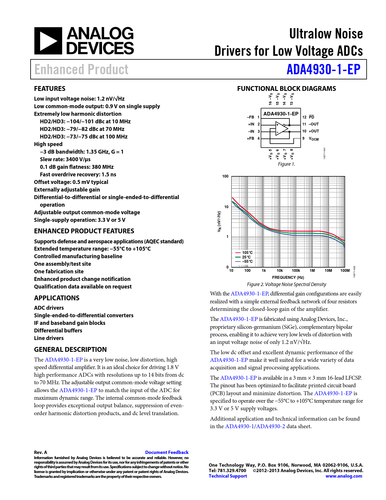
Ultralow Noise Drivers for Low Voltage ADCs Enhanced Product ADA4930-1-EP FEATURES FUNCTIONAL BLOCK DIAGRAMS S S S S Low input voltage noise: 1.2 nV/√Hz –V –V –V –V Low common-mode output: 0.9 V on single supply 16 15 14 13 Extremely low harmonic distortion ADA4930-1-EP –FB 1 12 PD HD2/HD3: −104/−101 dBc at 10 MHz +IN 2 11 –OUT HD2/HD3: −79/−82 dBc at 70 MHz –IN 3 10 +OUT HD2/HD3: −73/−75 dBc at 100 MHz +FB 4 9 VOCM High speed −3 dB bandwidth: 1.35 GHz, G = 1 5 6 7 8
001
S S S S Slew rate: 3400 V/µs +V +V +V +V
10371-
0.1 dB gain flatness: 380 MHz
Figure 1.
Fast overdrive recovery: 1.5 ns 100 Offset voltage: 0.5 mV typical Externally adjustable gain Differential-to-differential or single-ended-to-differential operation 10 Adjustable output common-mode voltage z) Single-supply operation: 3.3 V or 5 V √H V/ (n ENHANCED PRODUCT FEATURES NV 1 Supports defense and aerospace applications (AQEC standard) Extended temperature range: −55°C to +105°C 105°C Controlled manufacturing baseline 25°C One assembly/test site –55°C 0 One fabrication site
002
10 100 1k 10k 100k 1M 10M 100M Enhanced product change notification
10371-
FREQUENCY (Hz) Qualification data available on request
Figure 2. Voltage Noise Spectral Density With the ADA4930-1-EP, differential gain configurations are easily
APPLICATIONS
realized with a simple external feedback network of four resistors
ADC drivers
determining the closed-loop gain of the amplifier.
Single-ended-to-differential converters
The ADA4930-1-EP is fabricated using Analog Devices, Inc.,
IF and baseband gain blocks
proprietary silicon-germanium (SiGe), complementary bipolar
Differential buffers
process, enabling it to achieve very low levels of distortion with
Line drivers
an input voltage noise of only 1.2 nV/√Hz.
GENERAL DESCRIPTION
The low dc offset and excellent dynamic performance of the The ADA4930-1-EP is a very low noise, low distortion, high ADA4930-1-EP make it wel suited for a wide variety of data speed differential amplifier. It is an ideal choice for driving 1.8 V acquisition and signal processing applications. high performance ADCs with resolutions up to 14 bits from dc The ADA4930-1-EP is available in a 3 mm × 3 mm 16-lead LFCSP. to 70 MHz. The adjustable output common-mode voltage setting The pinout has been optimized to facilitate printed circuit board allows the ADA4930-1-EP to match the input of the ADC for (PCB) layout and minimize distortion. The ADA4930-1-EP is maximum dynamic range. The internal common-mode feedback specified to operate over the −55°C to +105°C temperature range for loop provides exceptional output balance, suppression of even- 3.3 V or 5 V supply voltages. order harmonic distortion products, and dc level translation. Additional application and technical information can be found in the ADA4930-1/ADA4930-2 data sheet.
Rev. A Document Feedback Information furnished by Analog Devices is believed to be accurate and reliable. However, no responsibility is assumed by Analog Devices for its use, nor for any infringements of patents or other rights of third parties that may result from its use. Specifications subject to change without notice. No One Technology Way, P.O. Box 9106, Norwood, MA 02062-9106, U.S.A. license is granted by implication or otherwise under any patent or patent rights of Analog Devices. Tel: 781.329.4700 ©2012–2013 Analog Devices, Inc. All rights reserved. Trademarks and registered trademarks are the property of their respective owners. Technical Support www.analog.com
Document Outline Features Enhanced Product Features Applications General Description Functional Block Diagrams Revision History Specifications 3.3 V Operation 3.3 V VOCM to VO, cm Performance 3.3 V General Performance 5 V Operation 5 V VOCM to VO, cm Performance 5 V General Performance Absolute Maximum Ratings Thermal Resistance Maximum Power Dissipation ESD Caution Pin Configuration and Function Descriptions Outline Dimensions Ordering Guide

 аккумуляторов")


