Datasheet ADL5501 (Analog Devices)
| Производитель | Analog Devices |
| Описание | 50 MHz TO 6 GHz TruPwr™ Detector |
| Страниц / Страница | 30 / 1 — 50 MHz to 6 GHz. TruPwr Detector. ADL5501. FEATURES |
| Версия | B |
| Формат / Размер файла | PDF / 2.0 Мб |
| Язык документа | английский |
50 MHz to 6 GHz. TruPwr Detector. ADL5501. FEATURES
Текстовая версия документа
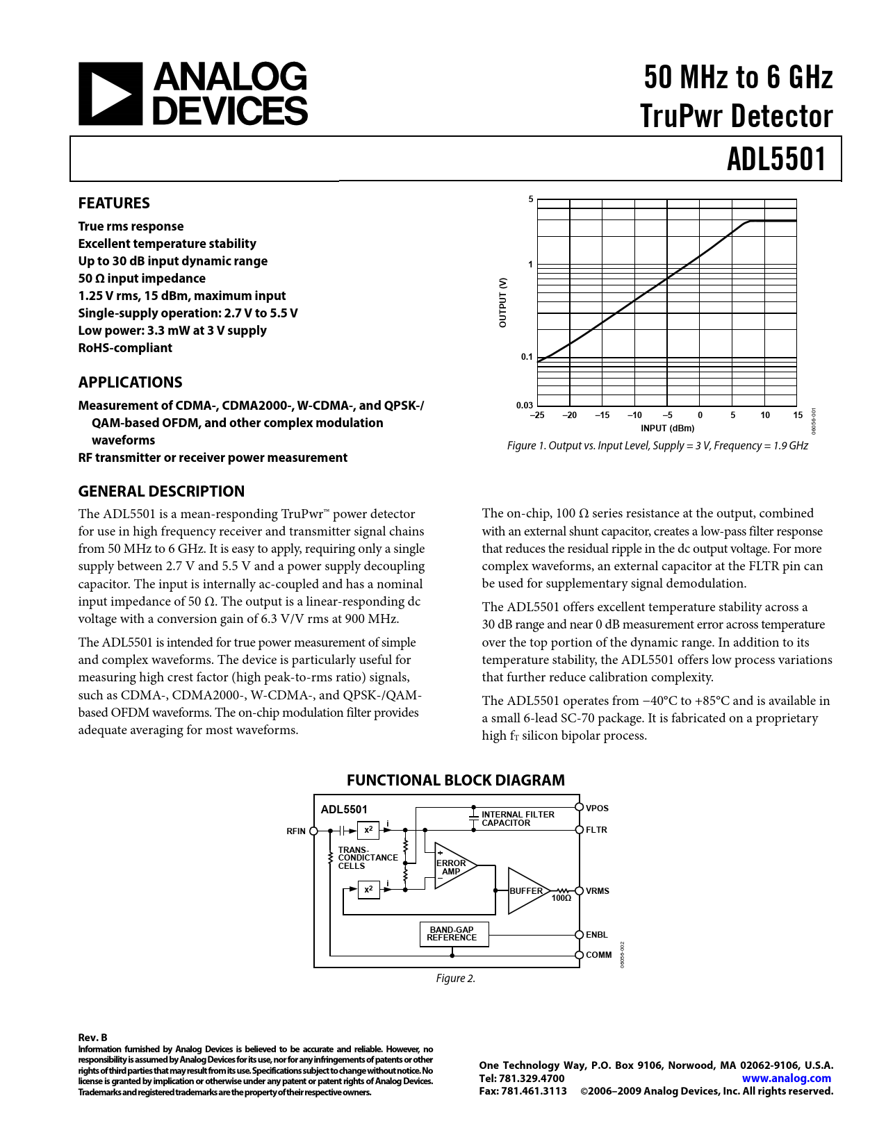
50 MHz to 6 GHz TruPwr Detector ADL5501 FEATURES 5 True rms response Excellent temperature stability Up to 30 dB input dynamic range 1 50 Ω input impedance ) V ( 1.25 V rms, 15 dBm, maximum input T U Single-supply operation: 2.7 V to 5.5 V TP OU Low power: 3.3 mW at 3 V supply RoHS-compliant 0.1 APPLICATIONS Measurement of CDMA-, CDMA2000-, W-CDMA-, and QPSK-/ 0.03
1
–25 –20 –15 –10 –5 0 5 10 15
00
QAM-based OFDM, and other complex modulation
6-
INPUT (dBm)
05 06
waveforms
Figure 1. Output vs. Input Level, Supply = 3 V, Frequency = 1.9 GHz
RF transmitter or receiver power measurement GENERAL DESCRIPTION
The ADL5501 is a mean-responding TruPwr™ power detector The on-chip, 100 Ω series resistance at the output, combined for use in high frequency receiver and transmitter signal chains with an external shunt capacitor, creates a low-pass filter response from 50 MHz to 6 GHz. It is easy to apply, requiring only a single that reduces the residual ripple in the dc output voltage. For more supply between 2.7 V and 5.5 V and a power supply decoupling complex waveforms, an external capacitor at the FLTR pin can capacitor. The input is internally ac-coupled and has a nominal be used for supplementary signal demodulation. input impedance of 50 Ω. The output is a linear-responding dc The ADL5501 offers excellent temperature stability across a voltage with a conversion gain of 6.3 V/V rms at 900 MHz. 30 dB range and near 0 dB measurement error across temperature The ADL5501 is intended for true power measurement of simple over the top portion of the dynamic range. In addition to its and complex waveforms. The device is particularly useful for temperature stability, the ADL5501 offers low process variations measuring high crest factor (high peak-to-rms ratio) signals, that further reduce calibration complexity. such as CDMA-, CDMA2000-, W-CDMA-, and QPSK-/QAM- The ADL5501 operates from −40°C to +85°C and is available in based OFDM waveforms. The on-chip modulation filter provides a small 6-lead SC-70 package. It is fabricated on a proprietary adequate averaging for most waveforms. high fT silicon bipolar process.
FUNCTIONAL BLOCK DIAGRAM VPOS ADL5501 INTERNAL FILTER i CAPACITOR RFIN x2 FLTR TRANS- CONDICTANCE ERROR CELLS AMP i x2 BUFFER VRMS 100Ω BAND-GAP REFERENCE ENBL
02
COMM
-0 6056 0 Figure 2.
Rev. B Information furnished by Analog Devices is believed to be accurate and reliable. However, no responsibility is assumed by Analog Devices for its use, nor for any infringements of patents or other One Technology Way, P.O. Box 9106, Norwood, MA 02062-9106, U.S.A. rights of third parties that may result from its use. Specifications subject to change without notice. No license is granted by implication or otherwise under any patent or patent rights of Analog Devices. Tel: 781.329.4700 www.analog.com Trademarks and registered trademarks are the property of their respective owners. Fax: 781.461.3113 ©2006–2009 Analog Devices, Inc. All rights reserved.
Document Outline FEATURES APPLICATIONS GENERAL DESCRIPTION FUNCTIONAL BLOCK DIAGRAM TABLE OF CONTENTS REVISION HISTORY SPECIFICATIONS ABSOLUTE MAXIMUM RATINGS ESD CAUTION PIN CONFIGURATION AND FUNCTION DESCRIPTIONS TYPICAL PERFORMANCE CHARACTERISTICS CIRCUIT DESCRIPTION FILTERING APPLICATIONS INFORMATION BASIC CONNECTIONS OUTPUT SWING LINEARITY INPUT COUPLING USING A SERIES RESISTOR MULTIPLE RF INPUTS SELECTING THE SQUARE-DOMAIN FILTER AND OUTPUT LOW-PASS FILTER POWER CONSUMPTION, ENABLE, AND POWER-ON/POWER-OFF RESPONSE TIME OUTPUT DRIVE CAPABILITY AND BUFFERING VRMS OUTPUT OFFSET DEVICE CALIBRATION AND ERROR CALCULATION CALIBRATION FOR IMPROVED ACCURACY DRIFT OVER A REDUCED TEMPERATURE RANGE OPERATION BELOW 100 MHz EVALUATION BOARD OUTLINE DIMENSIONS ORDERING GUIDE

 аккумуляторов")


