Datasheet MCP6V01, MCP6V02, MCP6V03 (Microchip)
| Производитель | Microchip |
| Описание | The MCP6V01/2/3 family of operational amplifiers has input offset voltage correction for very low offset and offset drift |
| Страниц / Страница | 44 / 1 — MCP6V01/2/3. 300 µA, Auto-Zeroed Op Amps. Features. Description. Package … |
| Формат / Размер файла | PDF / 1.0 Мб |
| Язык документа | английский |
MCP6V01/2/3. 300 µA, Auto-Zeroed Op Amps. Features. Description. Package Types (top view). MCP6V01. Typical Applications. MCP6V02
Модельный ряд для этого даташита
Текстовая версия документа
link to page 19
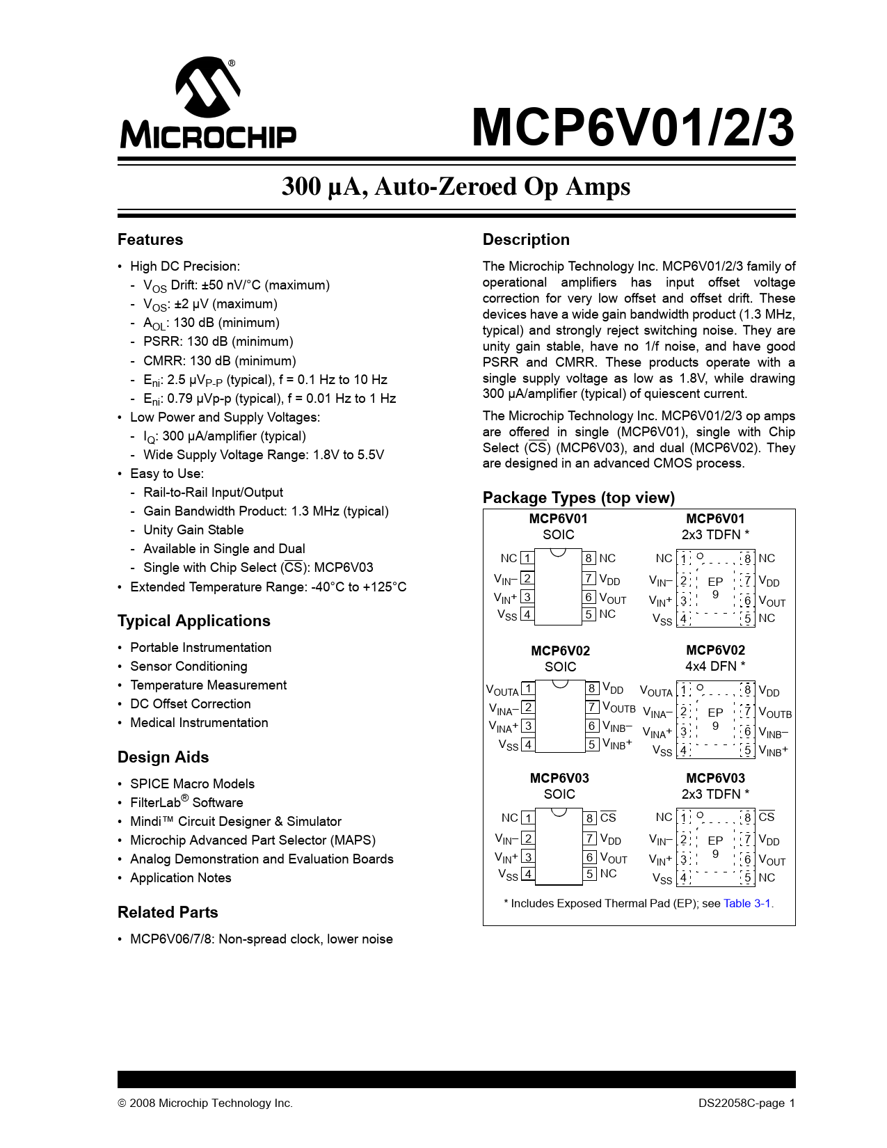
MCP6V01/2/3 300 µA, Auto-Zeroed Op Amps Features Description
• High DC Precision: The Microchip Technology Inc. MCP6V01/2/3 family of - V operational amplifiers has input offset voltage OS Drift: ±50 nV/°C (maximum) - V correction for very low offset and offset drift. These OS: ±2 µV (maximum) devices have a wide gain bandwidth product (1.3 MHz, - AOL: 130 dB (minimum) typical) and strongly reject switching noise. They are - PSRR: 130 dB (minimum) unity gain stable, have no 1/f noise, and have good - CMRR: 130 dB (minimum) PSRR and CMRR. These products operate with a - Eni: 2.5 µVP-P (typical), f = 0.1 Hz to 10 Hz single supply voltage as low as 1.8V, while drawing - E 300 µA/amplifier (typical) of quiescent current. ni: 0.79 µVp-p (typical), f = 0.01 Hz to 1 Hz • Low Power and Supply Voltages: The Microchip Technology Inc. MCP6V01/2/3 op amps - I are offered in single (MCP6V01), single with Chip Q: 300 µA/amplifier (typical) - Wide Supply Voltage Range: 1.8V to 5.5V Select (CS) (MCP6V03), and dual (MCP6V02). They are designed in an advanced CMOS process. • Easy to Use: - Rail-to-Rail Input/Output
Package Types (top view)
- Gain Bandwidth Product: 1.3 MHz (typical)
MCP6V01 MCP6V01
- Unity Gain Stable SOIC 2x3 TDFN * - Available in Single and Dual NC 1 8 NC NC 1 8 NC - Single with Chip Select (CS): MCP6V03 V 2 7 V • Extended Temperature Range: -40°C to +125°C IN– DD VIN– 2 EP 7 VDD V 9 IN+ 3 6 VOUT VIN+ 3 6 VOUT
Typical Applications
VSS 4 5 NC VSS 4 5 NC • Portable Instrumentation
MCP6V02 MCP6V02
• Sensor Conditioning SOIC 4x4 DFN * • Temperature Measurement V 1 8 V OUTA DD VOUTA 1 8 VDD • DC Offset Correction V V INA– 2 7 OUTB VINA– 2 EP 7 VOUTB • Medical Instrumentation VINA+ 3 6 VINB– V 9 INA+ 3 6 VINB– VSS 4 5 VINB+
Design Aids
VSS 4 5 VINB+ • SPICE Macro Models
MCP6V03 MCP6V03
SOIC 2x3 TDFN * • FilterLab® Software • Mindi™ Circuit Designer & Simulator NC 1 8 CS NC 1 8 CS • Microchip Advanced Part Selector (MAPS) VIN– 2 7 VDD VIN– 2 EP 7 VDD • Analog Demonstration and Evaluation Boards V 9 IN+ 3 6 VOUT VIN+ 3 6 VOUT • Application Notes VSS 4 5 NC VSS 4 5 NC
Related Parts
* Includes Exposed Thermal Pad (EP); see Table 3-1. • MCP6V06/7/8: Non-spread clock, lower noise © 2008 Microchip Technology Inc. DS22058C-page 1 Document Outline 1.0 Electrical Characteristics 1.1 Absolute Maximum Ratings † 1.2 Specifications TABLE 1-1: DC Electrical Specifications TABLE 1-2: AC Electrical Specifications TABLE 1-3: Digital Electrical Specifications TABLE 1-4: Temperature Specifications 1.3 Timing Diagrams FIGURE 1-1: Amplifier Start Up. FIGURE 1-2: Offset Correction Settling Time. FIGURE 1-3: Output Overdrive Recovery. FIGURE 1-4: Chip Select (MCP6V03). 1.4 Test Circuits FIGURE 1-5: AC and DC Test Circuit for Most Non-Inverting Gain Conditions. FIGURE 1-6: AC and DC Test Circuit for Most Inverting Gain Conditions. FIGURE 1-7: Test Circuit for Dynamic Input Behavior. 2.0 Typical Performance Curves 2.1 DC Input Precision FIGURE 2-1: Input Offset Voltage. FIGURE 2-2: Input Offset Voltage Drift. FIGURE 2-3: Input Offset Voltage Quadratic Temp Co. FIGURE 2-4: Input Offset Voltage vs. Power Supply Voltage with VCM = VCMR_L. FIGURE 2-5: Input Offset Voltage vs. Power Supply Voltage with VCM = VCMR_H. FIGURE 2-6: Input Offset Voltage vs. Output Voltage. FIGURE 2-7: Input Offset Voltage vs. Common Mode Voltage with VDD = 1.8V. FIGURE 2-8: Input Offset Voltage vs. Common Mode Voltage with VDD = 5.5V. FIGURE 2-9: CMRR. FIGURE 2-10: PSRR. FIGURE 2-11: DC Open-Loop Gain. FIGURE 2-12: CMRR and PSRR vs. Ambient Temperature. FIGURE 2-13: DC Open-Loop Gain vs. Ambient Temperature. FIGURE 2-14: Input Bias and Offset Currents vs. Common Mode Input Voltage with TA = +85˚C. FIGURE 2-15: Input Bias and Offset Currents vs. Common Mode Input Voltage with TA = +125˚C. FIGURE 2-16: Input Bias and Offset Currents vs. Ambient Temperature with VDD = +5.5V. FIGURE 2-17: Input Bias Current vs. Input Voltage (below VSS). 2.2 Other DC Voltages and Currents FIGURE 2-18: Input Common Mode Voltage Headroom (Range) vs. Ambient Temperature. FIGURE 2-19: Output Voltage Headroom vs. Output Current. FIGURE 2-20: Output Voltage Headroom vs. Ambient Temperature. FIGURE 2-21: Output Short Circuit Current vs. Power Supply Voltage. FIGURE 2-22: Supply Current vs. Power Supply Voltage. FIGURE 2-23: Power On Reset Trip Voltage. FIGURE 2-24: Power On Reset Voltage vs. Ambient Temperature. 2.3 Frequency Response FIGURE 2-25: CMRR and PSRR vs. Frequency. FIGURE 2-26: Open-Loop Gain vs. Frequency with VDD = 1.8V. FIGURE 2-27: Open-Loop Gain vs. Frequency with VDD = 5.5V. FIGURE 2-28: Gain Bandwidth Product and Phase Margin vs. Ambient Temperature. FIGURE 2-29: Gain Bandwidth Product and Phase Margin vs. Common Mode Input Voltage. FIGURE 2-30: Gain Bandwidth Product and Phase Margin vs. Output Voltage. FIGURE 2-31: Closed-Loop Output Impedance vs. Frequency with VDD = 1.8V. FIGURE 2-32: Closed-Loop Output Impedance vs. Frequency with VDD = 5.5V. FIGURE 2-33: Channel-to-Channel Separation vs. Frequency. FIGURE 2-34: Maximum Output Voltage Swing vs. Frequency. 2.4 Input Noise and Distortion FIGURE 2-35: Input Noise Voltage Density vs. Frequency. FIGURE 2-36: Input Noise Voltage Density vs. Input Common Mode Voltage. FIGURE 2-37: Inter-Modulation Distortion vs. Frequency with VCM Disturbance (see Figure 1-7). FIGURE 2-38: Inter-Modulation Distortion vs. Frequency with VDD Disturbance (see Figure 1-7). FIGURE 2-39: Input Noise vs. Time with 1 Hz and 10 Hz Filters and VDD =1.8V. FIGURE 2-40: Input Noise vs. Time with 1 Hz and 10 Hz Filters and VDD =5.5V. 2.5 Time Response FIGURE 2-41: Input Offset Voltage vs. Time with Temperature Change. FIGURE 2-42: Input Offset Voltage vs. Time at Power Up. FIGURE 2-43: The MCP6V01/2/3 family shows no input phase reversal with overdrive. FIGURE 2-44: Non-inverting Small Signal Step Response. FIGURE 2-45: Non-inverting Large Signal Step Response. FIGURE 2-46: Inverting Small Signal Step Response. FIGURE 2-47: Inverting Large Signal Step Response. FIGURE 2-48: Slew Rate vs. Ambient Temperature. FIGURE 2-49: Output Overdrive Recovery vs. Time with G = -100 V/V. FIGURE 2-50: Output Overdrive Recovery Time vs. Inverting Gain. 2.6 Chip Select Response (MCP6V03 only) FIGURE 2-51: Chip Select Current vs. Power Supply Voltage. FIGURE 2-52: Power Supply Current vs. Chip Select Voltage with VDD = 1.8V. FIGURE 2-53: Power Supply Current vs. Chip Select Voltage with VDD = 5.5V. FIGURE 2-54: Chip Select Current vs. Chip Select Voltage. FIGURE 2-55: Chip Select Voltage, Output Voltage vs. Time with VDD = 1.8V. FIGURE 2-56: Chip Select Voltage, Output Voltage vs. Time with VDD = 5.5V. FIGURE 2-57: Chip Select Relative Logic Thresholds vs. Ambient Temperature. FIGURE 2-58: Chip Select Hysteresis. FIGURE 2-59: Chip Select Turn On Time vs. Ambient Temperature. FIGURE 2-60: Chip Select’s Pull-down Resistor (RPD) vs. Ambient Temperature. FIGURE 2-61: Quiescent Current in Shutdown vs. Power Supply Voltage. 3.0 Pin Descriptions TABLE 3-1: Pin Function Table 3.1 Analog Outputs 3.2 Analog Inputs 3.3 Power Supply Pins 3.4 Chip Select (CS) Digital Input 3.5 Exposed Thermal Pad (EP) 4.0 Applications 4.1 Overview of Auto-zeroing Operation FIGURE 4-1: Simplified Auto-zeroed Op Amp Functional Diagram. FIGURE 4-2: Normal Mode of Operation (f1); Equivalent Amplifier Diagram. FIGURE 4-3: Auto-zeroing Mode of Operation (f2); Equivalent Diagram. 4.2 Other Functional Blocks FIGURE 4-4: Simplified Analog Input ESD Structures. FIGURE 4-5: Protecting the Analog Inputs. 4.3 Application Tips FIGURE 4-6: Output Resistor, RISO, Stabilizes Capacitive Loads. FIGURE 4-7: Recommended RISO values for Capacitive Loads. FIGURE 4-8: Output Load Issue. FIGURE 4-9: One Solution To Output Load Issue. FIGURE 4-10: Additional Supply Filtering. FIGURE 4-11: PCB Layout and Schematic for Single Non-inverting and Inverting Amplifiers. FIGURE 4-12: PCB Layout and Schematic for Single Difference Amplifier. FIGURE 4-13: PCB Layout and Schematic for Dual Non-inverting Amplifier. FIGURE 4-14: PCB Layout for Individual Resistors. 4.4 Typical Applications FIGURE 4-15: Simple Design. FIGURE 4-16: High Performance Design. FIGURE 4-17: RTD Sensor. FIGURE 4-18: Thermocouple Sensor; Simplified Circuit. FIGURE 4-19: Thermocouple Sensor. FIGURE 4-20: Offset Correction. FIGURE 4-21: Precision Comparator. 5.0 Design Aids 5.1 SPICE Macro Model 5.2 FilterLab® Software 5.3 Mindi™ Circuit Designer & Simulator 5.4 Microchip Advanced Part Selector (MAPS) 5.5 Analog Demonstration and Evaluation Boards 5.6 Application Notes 6.0 Packaging Information 6.1 Package Marking Information

 аккумуляторов")


