Datasheet MCP6N11 (Microchip)
| Производитель | Microchip |
| Описание | 500 kHz, 800 µA Instrumentation Amplifier |
| Страниц / Страница | 50 / 1 — MCP6N11. 500 kHz, 800 µA Instrumentation Amplifier. Features. … |
| Формат / Размер файла | PDF / 5.8 Мб |
| Язык документа | английский |
MCP6N11. 500 kHz, 800 µA Instrumentation Amplifier. Features. Description. Typical Applications. Typical Application Circuit
Модельный ряд для этого даташита
Текстовая версия документа
link to page 25
MCP6N11 500 kHz, 800 µA Instrumentation Amplifier Features Description
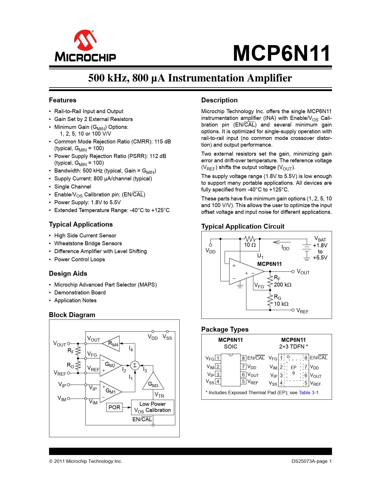
• Rail-to-Rail Input and Output Microchip Technology Inc. offers the single MCP6N11 • Gain Set by 2 External Resistors instrumentation amplifier (INA) with Enable/VOS Cali- • Minimum Gain (G bration pin (EN/CAL) and several minimum gain MIN) Options: 1, 2, 5, 10 or 100 V/V options. It is optimized for single-supply operation with rail-to-rail input (no common mode crossover distor- • Common Mode Rejection Ratio (CMRR): 115 dB tion) and output performance. (typical, GMIN = 100) • Power Supply Rejection Ratio (PSRR): 112 dB Two external resistors set the gain, minimizing gain (typical, G error and drift-over temperature. The reference voltage MIN = 100) (V • Bandwidth: 500 kHz (typical, Gain = G REF) shifts the output voltage (VOUT). MIN) • Supply Current: 800 μA/channel (typical) The supply voltage range (1.8V to 5.5V) is low enough to support many portable applications. All devices are • Single Channel fully specified from -40°C to +125°C. • Enable/VOS Calibration pin: (EN/CAL) These parts have five minimum gain options (1, 2, 5, 10 • Power Supply: 1.8V to 5.5V and 100 V/V). This allows the user to optimize the input • Extended Temperature Range: -40°C to +125°C offset voltage and input noise for different applications.
Typical Applications Typical Application Circuit
• High Side Current Sensor VBAT • Wheatstone Bridge Sensors 10 Ω I +1.8V • Difference Amplifier with Level Shifting V DD DD to U • Power Control Loops 1 +5.5V
MCP6N11 Design Aids
VOUT RF • Microchip Advanced Part Selector (MAPS) VFG 200 kΩ • Demonstration Board R • Application Notes G 10 kΩ V
Block Diagram
REF
Package Types
V V V DD SS OUT
MCP6N11 MCP6N11
VOUT RM4 SOIC 2×3 TDFN * R I F 4 VFG VFG 1 8 EN/CAL VFG 1 8 EN/CAL R G G V M2 Σ V 2 7 V V 2 EP 7 V REF I IM DD IM DD 2 I V 3 REF 9 I VIP 3 6 VOUT V 3 6 V 1 IP OUT V G VSS 4 5 VREF V 4 5 V IP M3 V SS REF IP GM1 V * Includes Exposed Thermal Pad (EP); see Table 3-1. TR VIM VIM Low Power POR VOS Calibration EN/CAL © 2011 Microchip Technology Inc. DS25073A-page 1 Document Outline 500 kHz, 800 µA Instrumentation Amplifier TABLE 1: Key Differentiating Specifications 1.0 Electrical Characteristics 1.1 Absolute Maximum Ratings † 1.2 Specifications TABLE 1-1: DC Electrical Specifications TABLE 1-2: AC Electrical Specifications TABLE 1-3: Digital Electrical Specifications TABLE 1-4: Temperature Specifications 1.3 Timing Diagrams FIGURE 1-1: Common Mode Input Overdrive Recovery Timing Diagram. FIGURE 1-2: Differential Mode Input Overdrive Recovery Timing Diagram. FIGURE 1-3: Output Overdrive Recovery Timing Diagram. FIGURE 1-4: POR Timing Diagram. FIGURE 1-5: EN/CAL Timing Diagram. 1.4 DC Test Circuits FIGURE 1-6: Test Circuit for Common Mode (Input Offset). TABLE 1-5: Selecting RF and RG FIGURE 1-7: Test Circuit for Differential Mode. TABLE 1-6: Selecting RF and RG 1.5 Explanation of DC Error Specs FIGURE 1-8: Input Offset Error vs. Common Mode Input Voltage. FIGURE 1-9: Differential Input Error vs. Differential Input Voltage. 2.0 Typical Performance Curves 2.1 DC Voltages and Currents FIGURE 2-1: Normalized Input Offset Voltage, with GMIN = 1 to 10. FIGURE 2-2: Normalized Input Offset Voltage, with GMIN = 100. FIGURE 2-3: Normalized Input Offset Voltage Drift, with GMIN = 1 to 10. FIGURE 2-4: Normalized Input Offset Voltage Drift, with GMIN = 100. FIGURE 2-5: Normalized Input Offset Voltage vs. Power Supply Voltage, with VCM = 0V and GMIN = 1 to 10. FIGURE 2-6: Normalized Input Offset Voltage vs. Power Supply Voltage, with VCM = 0V and GMIN = 100. FIGURE 2-7: Normalized Input Offset Voltage vs. Power Supply Voltage, with VCM = VDD and GMIN = 1 to 10. FIGURE 2-8: Normalized Input Offset Voltage vs. Power Supply Voltage, with VCM = VDD and GMIN = 100. FIGURE 2-9: Normalized Input Offset Voltage vs. Output Voltage, with GMIN = 1 to 10. FIGURE 2-10: Normalized Input Offset Voltage vs. Output Voltage, with GMIN = 100. FIGURE 2-11: Input Common Mode Voltage Headroom vs. Ambient Temperature. FIGURE 2-12: Normalized Input Offset Voltage vs. Common Mode Voltage, with VDD = 1.8V and GMIN = 1 to 10. FIGURE 2-13: Normalized Input Offset Voltage vs. Common Mode Voltage, with VDD = 1.8V and GMIN = 100. FIGURE 2-14: Normalized Input Offset Voltage vs. Common Mode Voltage, with VDD = 5.5V and GMIN = 1 to 10. FIGURE 2-15: Normalized Input Offset Voltage vs. Common Mode Voltage, with VDD = 5.5V and GMIN = 100. FIGURE 2-16: Normalized CMRR and PSRR vs. Ambient Temperature. FIGURE 2-17: Normalized DC Open-Loop Gain vs. Ambient Temperature. FIGURE 2-18: The MCP6N11 Shows No Phase Reversal vs. Common Mode Voltage. FIGURE 2-19: Normalized Differential Mode Voltage Range vs. Ambient Temperature. FIGURE 2-20: Normalized Differential Input Error vs. Differential Voltage, with GMIN = 1. FIGURE 2-21: Normalized Differential Input Error vs. Differential Voltage, with GMIN = 2 to 100. FIGURE 2-22: The MCP6N11 Shows No Phase Reversal vs. Differential Voltage, with VDD = 5.5V. FIGURE 2-23: Input Bias and Offset Currents vs. Ambient Temperature, with VDD = +5.5V. FIGURE 2-24: Input Bias Current vs. Input Voltage (below VSS). FIGURE 2-25: Input Bias and Offset Currents vs. Common Mode Input Voltage, with TA = +85°C. FIGURE 2-26: Input Bias and Offset Currents vs. Common Mode Input Voltage, with TA = +125°C. FIGURE 2-27: Output Voltage Headroom vs. Output Current. FIGURE 2-28: Output Voltage Headroom vs. Ambient Temperature. FIGURE 2-29: Output Short Circuit Current vs. Power Supply Voltage. FIGURE 2-30: Supply Current vs. Power Supply Voltage. FIGURE 2-31: Supply Current vs. Common Mode Input Voltage. 2.2 Frequency Response FIGURE 2-32: CMRR vs. Frequency. FIGURE 2-33: PSRR vs. Frequency. FIGURE 2-34: Normalized Open-Loop Gain vs. Frequency. FIGURE 2-35: Normalized Gain Bandwidth Product and Phase Margin vs. Ambient Temperature. FIGURE 2-36: Closed-Loop Output Impedance vs. Frequency. FIGURE 2-37: Gain Peaking vs. Normalized Capacitive Load. 2.3 Noise FIGURE 2-38: Normalized Input Noise Voltage Density vs. Frequency. FIGURE 2-39: Normalized Input Noise Voltage Density vs. Input Common Mode Voltage, with f = 100 Hz. FIGURE 2-40: Normalized Input Noise Voltage Density vs. Input Common Mode Voltage, with f = 10 kHz. FIGURE 2-41: Normalized Input Noise Voltage vs. Time, with GMIN = 1 to 10. FIGURE 2-42: Normalized Input Noise Voltage vs. Time, with GMIN = 100. 2.4 Time Response FIGURE 2-43: Small Signal Step Response. FIGURE 2-44: Large Signal Step Response. FIGURE 2-45: Slew Rate vs. Ambient Temperature. FIGURE 2-46: Maximum Output Voltage Swing vs. Frequency. FIGURE 2-47: Common Mode Input Overdrive Recovery Time vs. Normalized Gain. FIGURE 2-48: Differential Input Overdrive Recovery Time vs. Normalized Gain. FIGURE 2-49: Output Overdrive Recovery Time vs. Normalized Gain. FIGURE 2-50: The MCP6N11 Shows No Phase Reversal vs. Common Mode Input Overdrive, with VDD = 5.5V. FIGURE 2-51: The MCP6N11 Shows No Phase Reversal vs. Differential Input Overdrive, with VDD = 5.5V. 2.5 Enable/Calibration and POR Responses FIGURE 2-52: EN/CAL and Output Voltage vs. Time, with VDD = 1.8V. FIGURE 2-53: EN/CAL and Output Voltage vs. Time, with VDD = 5.5V FIGURE 2-54: EN/CAL Hysteresis vs. Ambient Temperature. FIGURE 2-55: EN/CAL Turn On Time vs. Ambient Temperature. FIGURE 2-56: Power Supply On and Off and Output Voltage vs. Time. FIGURE 2-57: POR Trip Voltages and Hysteresis vs. Temperature. FIGURE 2-58: Quiescent Current in Shutdown vs. Power Supply Voltage. FIGURE 2-59: Output Leakage Current vs. Output Voltage. 3.0 Pin Descriptions TABLE 3-1: Pin Function Table 3.1 Analog Signal Inputs 3.2 Analog Feedback Input 3.3 Analog Reference Input 3.4 Analog Output 3.5 Power Supply Pins 3.6 Digital Enable and VOS Calibration Input 3.7 Exposed Thermal Pad (EP) 4.0 Applications 4.1 Basic Performance FIGURE 4-1: Standard Circuit. FIGURE 4-2: MCP6N11 Block Diagram. FIGURE 4-3: DC Bias Resistors. 4.2 Functional Blocks FIGURE 4-4: Simplified Analog Input ESD Structures. FIGURE 4-5: Protecting the Analog Inputs Against High Voltages. FIGURE 4-6: Protecting the Analog Inputs Against High Currents. FIGURE 4-7: Input Voltage Ranges. 4.3 Applications Tips FIGURE 4-8: Output Resistor, RISO stabilizes large capacitive loads. FIGURE 4-9: Recommended RISO Values for Capacitive Loads. FIGURE 4-10: Simple Gain Circuit with Parasitic Capacitances. 4.4 Typical Applications FIGURE 4-11: Difference Amplifier. FIGURE 4-12: Difference Amplifier with Very Large Common Mode Component. FIGURE 4-13: High Side Current Detector. FIGURE 4-14: Wheatstone Bridge Amplifier. 5.0 Design Aids 5.1 Microchip Advanced Part Selector (MAPS) 5.2 Analog Demonstration Board 5.3 Application Notes 6.0 Packaging Information 6.1 Package Marking Information Appendix A: Revision History Revision A (October 2011) Product Identification System Trademarks Worldwide Sales and Service

 аккумуляторов")


