Datasheet AD8370 (Analog Devices)
| Производитель | Analog Devices |
| Описание | 750 MHz Digitally Controlled Variable Gain Amplifier |
| Страниц / Страница | 28 / 1 — LF to 750 MHz,. Digitally Controlled VGA. Data Sheet. AD8370. FEATURES. … |
| Версия | B |
| Формат / Размер файла | PDF / 786 Кб |
| Язык документа | английский |
LF to 750 MHz,. Digitally Controlled VGA. Data Sheet. AD8370. FEATURES. FUNCTIONAL BLOCK DIAGRAM
Модельный ряд для этого даташита
Текстовая версия документа
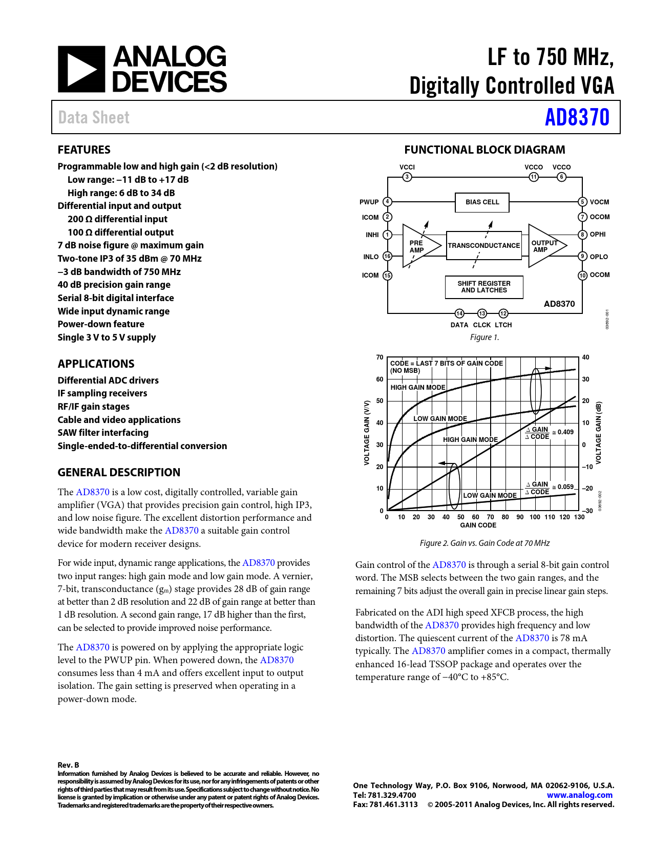
LF to 750 MHz, Digitally Controlled VGA Data Sheet AD8370 FEATURES FUNCTIONAL BLOCK DIAGRAM Programmable low and high gain (<2 dB resolution) VCCI VCCO VCCO Low range: −11 dB to +17 dB 3 11 6 High range: 6 dB to 34 dB Differential input and output PWUP 4 BIAS CELL 5 VOCM 200 Ω differential input ICOM 2 7 OCOM 100 Ω differential output INHI 1 8 OPHI 7 dB noise figure @ maximum gain PRE TRANSCONDUCTANCE OUTPUT AMP AMP Two-tone IP3 of 35 dBm @ 70 MHz INLO 16 9 OPLO −3 dB bandwidth of 750 MHz ICOM 15 10 OCOM 40 dB precision gain range SHIFT REGISTER AND LATCHES Serial 8-bit digital interface AD8370 Wide input dynamic range 14 13 12 Power-down feature DATA CLCK LTCH
03692-001
Single 3 V to 5 V supply
Figure 1.
70 40 APPLICATIONS CODE = LAST 7 BITS OF GAIN CODE (NO MSB) Differential ADC drivers 60 30 HIGH GAIN MODE IF sampling receivers 50 20 RF/IF gain stages /V) B) V d Cable and video applications LOW GAIN MODE 40 10
SAW filter interfacing GAIN
0.409
CODE HIGH GAIN MODE Single-ended-to-differential conversion 30 0 VOLTAGE GAIN ( VOLTAGE GAIN ( 20 –10 GENERAL DESCRIPTION
GAIN
0.059
The AD8370 is a low cost, digitally controlled, variable gain
10 –20
CODE LOW GAIN MODE
amplifier (VGA) that provides precision gain control, high IP3,
0 –30
03692-002 and low noise figure. The excellent distortion performance and
0 10 20 30 40 50 60 70 80 90 100 110 120 130 GAIN CODE
wide bandwidth make the AD8370 a suitable gain control device for modern receiver designs. Figure 2. Gain vs. Gain Code at 70 MHz For wide input, dynamic range applications, the AD8370 provides Gain control of the AD8370 is through a serial 8-bit gain control two input ranges: high gain mode and low gain mode. A vernier, word. The MSB selects between the two gain ranges, and the 7-bit, transconductance (gm) stage provides 28 dB of gain range remaining 7 bits adjust the overall gain in precise linear gain steps. at better than 2 dB resolution and 22 dB of gain range at better than 1 dB resolution. A second gain range, 17 dB higher than the first, Fabricated on the ADI high speed XFCB process, the high can be selected to provide improved noise performance. bandwidth of the AD8370 provides high frequency and low distortion. The quiescent current of the AD8370 is 78 mA The AD8370 is powered on by applying the appropriate logic typically. The AD8370 amplifier comes in a compact, thermally level to the PWUP pin. When powered down, the AD8370 enhanced 16-lead TSSOP package and operates over the consumes less than 4 mA and offers excellent input to output temperature range of −40°C to +85°C. isolation. The gain setting is preserved when operating in a power-down mode.
Rev. B Information furnished by Analog Devices is believed to be accurate and reliable. However, no responsibility is assumed by Analog Devices for its use, nor for any infringements of patents or other One Technology Way, P.O. Box 9106, Norwood, MA 02062-9106, U.S.A. rights of third parties that may result from its use. Specifications subject to change without notice. No license is granted by implication or otherwise under any patent or patent rights of Analog Devices. Tel: 781.329.4700 www.analog.com Trademarks and registered trademarks are the property of their respective owners. Fax: 781.461.3113 © 2005-2011 Analog Devices, Inc. All rights reserved.
Document Outline Features Applications General Description Functional Block Diagram Table of Contents Revision History Specifications Absolute Maximum Ratings ESD Caution Pin Configuration and Function Descriptions Typical Performance Characteristics Theory of Operation Block Architecture Preamplifier Transconductance Stage Output Amplifier Digital Interface and Timing Applications Basic Connections Gain Codes Power-Up Feature Choosing Between Gain Ranges Layout and Operating Considerations Package Considerations Single-Ended-to-Differential Conversion DC-Coupled Operation ADC Interfacing 3 V Operation Evaluation Board and Software Appendix Characterization Equipment Composite Waveform Assumption Definitions of Selected Parameters Outline Dimensions Ordering Guide

 аккумуляторов")


