DatasheetsDatasheet ADSP-BF522, ADSP-BF523, ADSP-BF524, …
Datasheet ADSP-BF522, ADSP-BF523, ADSP-BF524, ADSP-BF525, ADSP-BF526, ADSP-BF527 (Analog Devices)
| Производитель | Analog Devices |
| Описание | Blackfin Embedded Processor |
| Страниц / Страница | 88 / 1 — Blackfin. Embedded Processor. ADSP-BF522/ADSP-BF523/ADSP-BF524/. … |
| Версия | D |
| Формат / Размер файла | PDF / 3.0 Мб |
| Язык документа | английский |
Blackfin. Embedded Processor. ADSP-BF522/ADSP-BF523/ADSP-BF524/. ADSP-BF525/ADSP-BF526/ADSP-BF527. FEATURES. PERIPHERALS
Модельный ряд для этого даташита
Текстовая версия документа
link to page 28 link to page 3 link to page 87 link to page 87
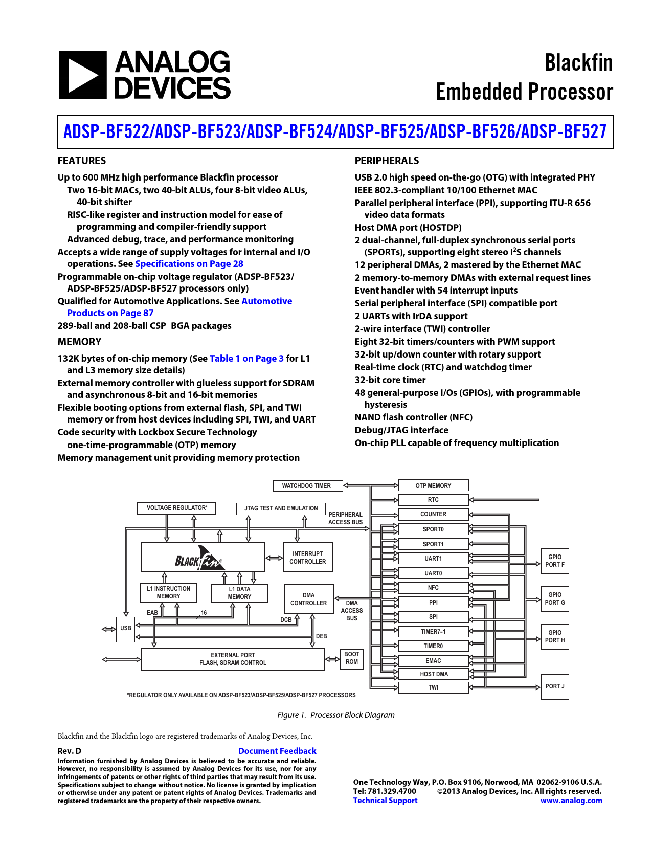
Blackfin Embedded Processor ADSP-BF522/ADSP-BF523/ADSP-BF524/ ADSP-BF525/ADSP-BF526/ADSP-BF527 FEATURES PERIPHERALS Up to 600 MHz high performance Blackfin processor USB 2.0 high speed on-the-go (OTG) with integrated PHY Two 16-bit MACs, two 40-bit ALUs, four 8-bit video ALUs, IEEE 802.3-compliant 10/100 Ethernet MAC 40-bit shifter Parallel peripheral interface (PPI), supporting ITU-R 656 RISC-like register and instruction model for ease of video data formats programming and compiler-friendly support Host DMA port (HOSTDP) Advanced debug, trace, and performance monitoring 2 dual-channel, full-duplex synchronous serial ports Accepts a wide range of supply voltages for internal and I/O (SPORTs), supporting eight stereo I2S channels operations. See Specifications on Page 28 12 peripheral DMAs, 2 mastered by the Ethernet MAC Programmable on-chip voltage regulator (ADSP-BF523/ 2 memory-to-memory DMAs with external request lines ADSP-BF525/ADSP-BF527 processors only) Event handler with 54 interrupt inputs Qualified for Automotive Applications. See Automotive Serial peripheral interface (SPI) compatible port Products on Page 87 2 UARTs with IrDA support 289-ball and 208-ball CSP_BGA packages 2-wire interface (TWI) controller MEMORY Eight 32-bit timers/counters with PWM support 132K bytes of on-chip memory (See Table 1 on Page 3 for L1 32-bit up/down counter with rotary support and L3 memory size details) Real-time clock (RTC) and watchdog timer External memory controller with glueless support for SDRAM 32-bit core timer and asynchronous 8-bit and 16-bit memories 48 general-purpose I/Os (GPIOs), with programmable Flexible booting options from external flash, SPI, and TWI hysteresis memory or from host devices including SPI, TWI, and UART NAND flash controller (NFC) Code security with Lockbox Secure Technology Debug/JTAG interface one-time-programmable (OTP) memory On-chip PLL capable of frequency multiplication Memory management unit providing memory protection WATCHDOG TIMER OTP MEMORY RTC VOLTAGE REGULATOR* JTAG TEST AND EMULATION PERIPHERAL COUNTER ACCESS BUS SPORT0 SPORT1 INTERRUPT UART1 GPIO
B
CONTROLLER PORT F UART0 L1 INSTRUCTION L1 DATA NFC MEMORY DMA GPIO MEMORY CONTROLLER DMA PPI PORT G EAB ACCESS 16 SPI DCB BUS USB TIMER7-1 GPIO DEB PORT H TIMER0 EXTERNAL PORT BOOT FLASH, SDRAM CONTROL ROM EMAC HOST DMA TWI PORT J *REGULATOR ONLY AVAILABLE ON ADSP-BF523/ADSP-BF525/ADSP-BF527 PROCESSORS
Figure 1. Processor Block Diagram Blackfin and the Blackfin logo are registered trademarks of Analog Devices, Inc.
Rev. D Do cument Feedback Information furnished by Analog Devices is believed to be accurate and reliable. However, no responsibility is assumed by Analog Devices for its use, nor for any infringements of patents or other rights of third parties that may result from its use. Specifications subject to change without notice. No license is granted by implication One Technology Way, P.O. Box 9106, Norwood, MA 02062-9106 U.S.A. or otherwise under any patent or patent rights of Analog Devices. Trademarks and Tel: 781.329.4700 ©2013 Analog Devices, Inc. All rights reserved. registered trademarks are the property of their respective owners. Technical Support www.analog.com
Document Outline Blackfin Embedded Processor Features Memory Peripherals Table Of Contents Revision History General Description Portable Low Power Architecture System Integration Processor Peripherals Blackfin Processor Core Memory Architecture Internal (On-Chip) Memory External (Off-Chip) Memory NAND Flash Controller (NFC) One-Time Programmable Memory I/O Memory Space Booting Event Handling Core Event Controller (CEC) System Interrupt Controller (SIC) Event Control DMA Controllers Host DMA Port Real-Time Clock Watchdog Timer Timers Up/Down Counter and Thumbwheel Interface Serial Ports Serial Peripheral Interface (SPI) Port UART Ports TWI Controller Interface 10/100 Ethernet MAC Ports General-Purpose I/O (GPIO) Parallel Peripheral Interface (PPI) General-Purpose Mode Descriptions Input Mode Frame Capture Mode Output Mode ITU-R 656 Mode Descriptions Active Video Mode Vertical Blanking Interval Mode Entire Field Mode USB On-The-Go Dual-Role Device Controller Code Security with Lockbox Secure Technology Dynamic Power Management Full-On Operating Mode—Maximum Performance Active Operating Mode—Moderate Dynamic Power Savings Sleep Operating Mode—High Dynamic Power Savings Deep Sleep Operating Mode—Maximum Dynamic Power Savings Hibernate State—Maximum Static Power Savings Power Savings ADSP-BF523/ADSP-BF525/ADSP-BF527 Voltage Regulation ADSP-BF522/ADSP-BF524/ADSP-BF526 Voltage Regulation Clock Signals Booting Modes Instruction Set Description Development Tools Integrated Development Environments (IDEs) EZ-KIT Lite Evaluation Board EZ-KIT Lite Evaluation Kits Software Add-Ins for CrossCore Embedded Studio Board Support Packages for Evaluation Hardware Middleware Packages Algorithmic Modules Designing an Emulator-Compatible DSP Board (Target) Additional Information Related Signal Chains Lockbox Secure Technology Disclaimer Signal Descriptions Specifications Operating Conditions for ADSP-BF522/ADSP-BF524/ADSP-BF526 Processors Clock Related Operating Conditions for ADSP-BF522/ADSP-BF524/ADSP-BF526 Processors Operating Conditions for ADSP-BF523/ADSP-BF525/ADSP-BF527 Processors Clock Related Operating Conditions for ADSP-BF523/ADSP-BF525/ADSP-BF527 Processors Electrical Characteristics Total Power Dissipation Absolute Maximum Ratings Package Information ESD Sensitivity Timing Specifications Clock and Reset Timing Asynchronous Memory Read Cycle Timing Asynchronous Memory Write Cycle Timing NAND Flash Controller Interface Timing SDRAM Interface Timing External DMA Request Timing Parallel Peripheral Interface Timing Serial Ports Serial Peripheral Interface (SPI) Port—Master Timing Serial Peripheral Interface (SPI) Port—Slave Timing Universal Serial Bus (USB) On-The-Go—Receive and Transmit Timing Universal Asynchronous Receiver-Transmitter (UART) Ports—Receive and Transmit Timing General-Purpose Port Timing Timer Cycle Timing Timer Clock Timing Up/Down Counter/Rotary Encoder Timing HOSTDP A/C Timing- Host Read Cycle HOSTDP A/C Timing- Host Write Cycle 10/100 Ethernet MAC Controller Timing JTAG Test And Emulation Port Timing Output Drive Currents Test Conditions Output Enable Time Measurement Output Disable Time Measurement Example System Hold Time Calculation Capacitive Loading Environmental Conditions 289-Ball CSP_BGA Ball Assignment 208-Ball CSP_BGA Ball Assignment Outline Dimensions Surface-Mount Design Automotive Products Ordering Guide

 аккумуляторов")


