Datasheet AD7923-EP (Analog Devices)
| Производитель | Analog Devices |
| Описание | 4-Channel 200 kSPS, 12-Bit A/D Converter with Sequencer in 16-Lead TSSOP |
| Страниц / Страница | 9 / 1 — 4-Channel, 200 kSPS 12-Bit ADC. with Sequencer in 16-Lead TSSOP. Enhanced … |
| Версия | A |
| Формат / Размер файла | PDF / 305 Кб |
| Язык документа | английский |
4-Channel, 200 kSPS 12-Bit ADC. with Sequencer in 16-Lead TSSOP. Enhanced Product. AD7923-EP. FEATURES. FUNCTIONAL BLOCK DIAGRAM
Модельный ряд для этого даташита
Текстовая версия документа
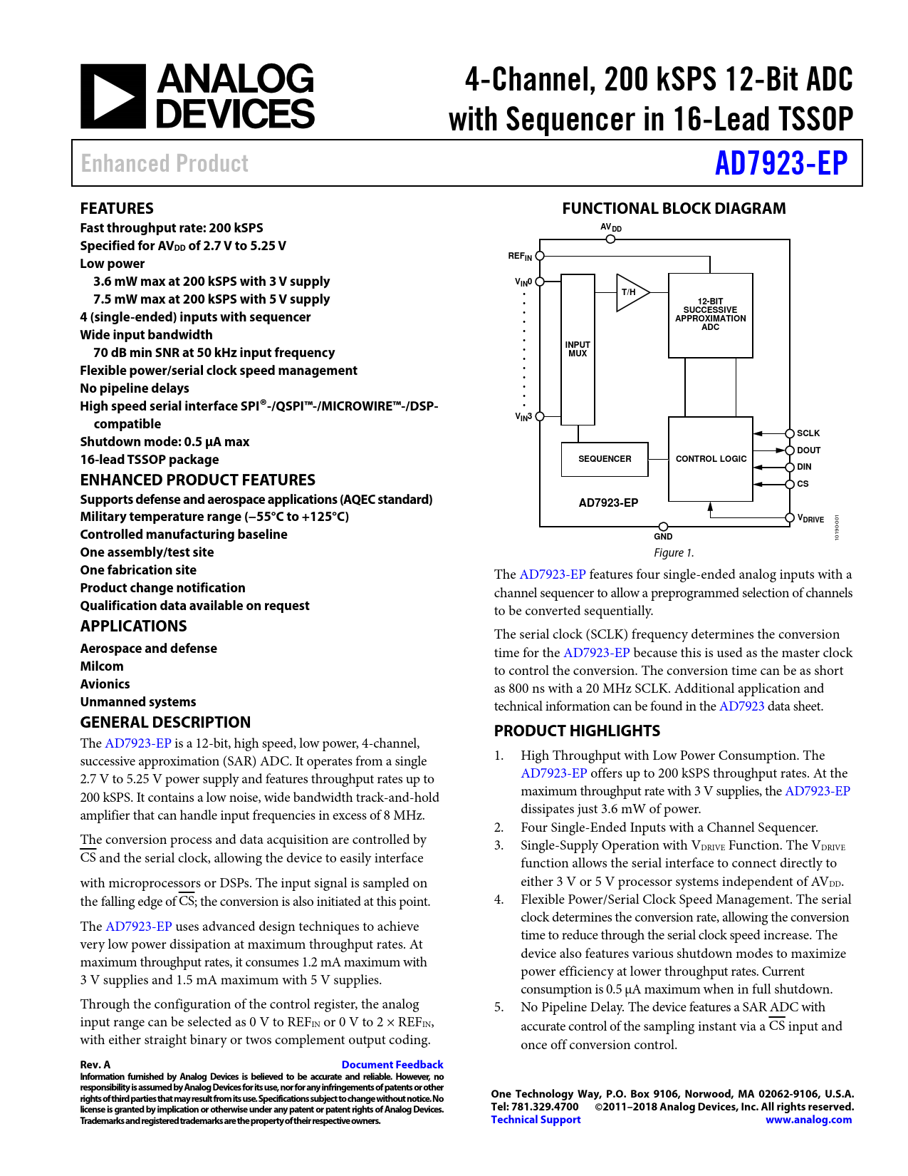
4-Channel, 200 kSPS 12-Bit ADC with Sequencer in 16-Lead TSSOP Enhanced Product AD7923-EP FEATURES FUNCTIONAL BLOCK DIAGRAM Fast throughput rate: 200 kSPS AVDD Specified for AVDD of 2.7 V to 5.25 V REF Low power IN 3.6 mW max at 200 kSPS with 3 V supply VIN0 T/H 7.5 mW max at 200 kSPS with 5 V supply • • 12-BIT SUCCESSIVE 4 (single-ended) inputs with sequencer • • APPROXIMATION ADC Wide input bandwidth • • INPUT 70 dB min SNR at 50 kHz input frequency • MUX • Flexible power/serial clock speed management • • No pipeline delays • • High speed serial interface SPI®-/QSPI™-/MICROWIRE™-/DSP- • V compatible IN3 SCLK Shutdown mode: 0.5 μA max DOUT 16-lead TSSOP package SEQUENCER CONTROL LOGIC DIN ENHANCED PRODUCT FEATURES CS Supports defense and aerospace applications (AQEC standard) AD7923-EP Military temperature range (−55°C to +125°C) VDRIVE
01 0 0-
Controlled manufacturing baseline
19
GND
10
One assembly/test site
Figure 1.
One fabrication site
The AD7923-EP features four single-ended analog inputs with a
Product change notification
channel sequencer to allow a preprogrammed selection of channels
Qualification data available on request
to be converted sequentially.
APPLICATIONS
The serial clock (SCLK) frequency determines the conversion
Aerospace and defense
time for the AD7923-EP because this is used as the master clock
Milcom
to control the conversion. The conversion time can be as short
Avionics
as 800 ns with a 20 MHz SCLK. Additional application and
Unmanned systems
technical information can be found in the AD7923 data sheet.
GENERAL DESCRIPTION PRODUCT HIGHLIGHTS
The AD7923-EP is a 12-bit, high speed, low power, 4-channel, successive approximation (SAR) ADC. It operates from a single 1. High Throughput with Low Power Consumption. The 2.7 V to 5.25 V power supply and features throughput rates up to AD7923-EP offers up to 200 kSPS throughput rates. At the 200 kSPS. It contains a low noise, wide bandwidth track-and-hold maximum throughput rate with 3 V supplies, the AD7923-EP amplifier that can handle input frequencies in excess of 8 MHz. dissipates just 3.6 mW of power. 2. Four Single-Ended Inputs with a Channel Sequencer. The conversion process and data acquisition are controlled by 3. Single-Supply Operation with VDRIVE Function. The VDRIVE CS and the serial clock, allowing the device to easily interface function allows the serial interface to connect directly to with microprocessors or DSPs. The input signal is sampled on either 3 V or 5 V processor systems independent of AVDD. the falling edge of CS; the conversion is also initiated at this point. 4. Flexible Power/Serial Clock Speed Management. The serial clock determines the conversion rate, allowing the conversion The AD7923-EP uses advanced design techniques to achieve time to reduce through the serial clock speed increase. The very low power dissipation at maximum throughput rates. At device also features various shutdown modes to maximize maximum throughput rates, it consumes 1.2 mA maximum with power efficiency at lower throughput rates. Current 3 V supplies and 1.5 mA maximum with 5 V supplies. consumption is 0.5 μA maximum when in full shutdown. Through the configuration of the control register, the analog 5. No Pipeline Delay. The device features a SAR ADC with input range can be selected as 0 V to REFIN or 0 V to 2 × REFIN, accurate control of the sampling instant via a CS input and with either straight binary or twos complement output coding. once off conversion control.
Rev. A Document Feedback Information furnished by Analog Devices is believed to be accurate and reliable. However, no responsibility is assumed by Analog Devices for its use, nor for any infringements of patents or other rights of third parties that may result from its use. Specifications subject to change without notice. No One Technology Way, P.O. Box 9106, Norwood, MA 02062-9106, U.S.A. license is granted by implication or otherwise under any patent or patent rights of Analog Devices. Tel: 781.329.4700 ©2011–2018 Analog Devices, Inc. All rights reserved. Trademarks and registered trademarks are the property of their respective owners. Technical Support www.analog.com
Document Outline Features Enhanced Product Features Applications General Description Functional Block Diagram Product Highlights Table of Contents Revision History Specifications Timing Specifications Absolute Maximum Ratings ESD Caution Pin Configuration and Function Description Typical Performance Characteristics Outline Dimensions Ordering Guide

 аккумуляторов")


