Datasheet AD4003-KGD (Analog Devices) - 4
| Производитель | Analog Devices |
| Описание | 18-Bit, 2 MSPS, Easy Drive, Differential SAR ADC |
| Страниц / Страница | 9 / 4 — AD4003-KGD. Known Good Die. Parameter. Test Conditions/Comments. Min. … |
| Формат / Размер файла | PDF / 240 Кб |
| Язык документа | английский |
AD4003-KGD. Known Good Die. Parameter. Test Conditions/Comments. Min. Typ. Max. Unit
Модельный ряд для этого даташита
Текстовая версия документа
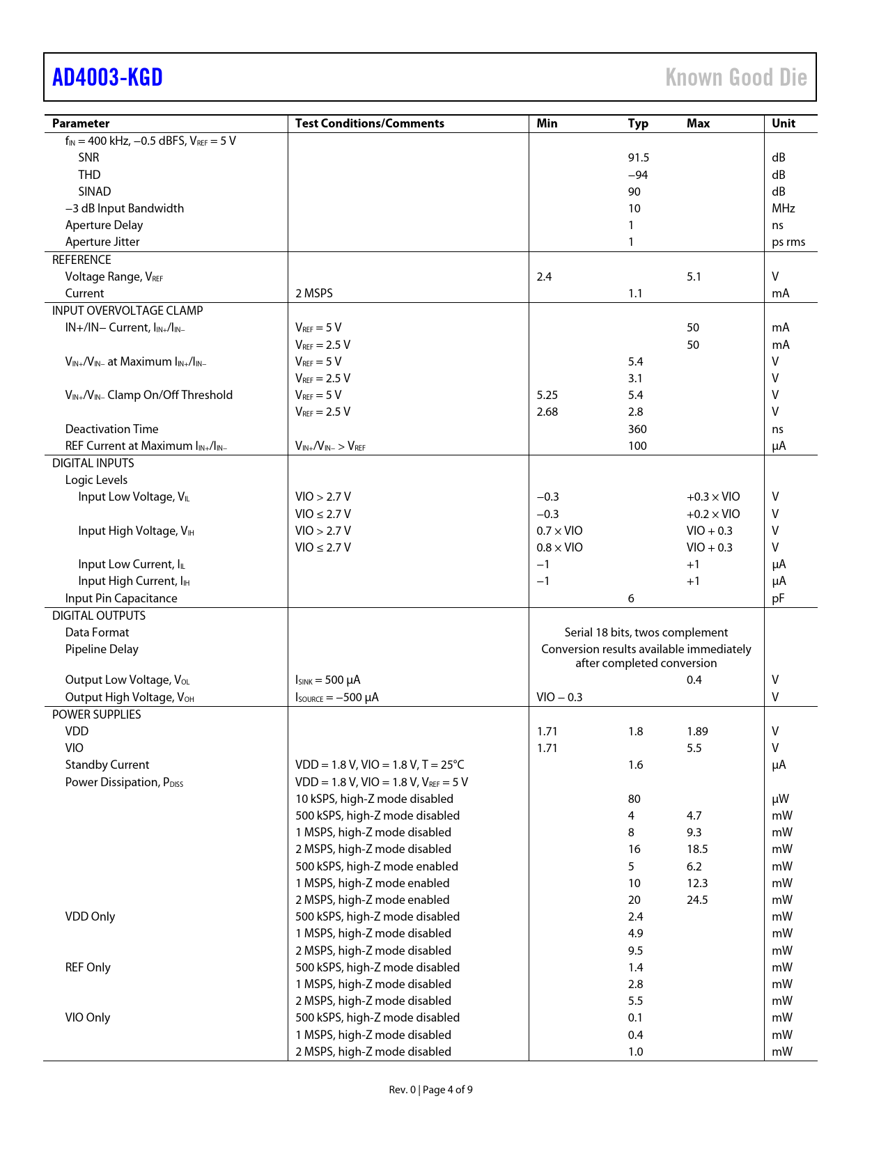
AD4003-KGD Known Good Die Parameter Test Conditions/Comments Min Typ Max Unit
fIN = 400 kHz, −0.5 dBFS, VREF = 5 V SNR 91.5 dB THD −94 dB SINAD 90 dB −3 dB Input Bandwidth 10 MHz Aperture Delay 1 ns Aperture Jitter 1 ps rms REFERENCE Voltage Range, VREF 2.4 5.1 V Current 2 MSPS 1.1 mA INPUT OVERVOLTAGE CLAMP IN+/IN− Current, IIN+/IIN− VREF = 5 V 50 mA VREF = 2.5 V 50 mA VIN+/VIN− at Maximum IIN+/IIN− VREF = 5 V 5.4 V VREF = 2.5 V 3.1 V VIN+/VIN− Clamp On/Off Threshold VREF = 5 V 5.25 5.4 V VREF = 2.5 V 2.68 2.8 V Deactivation Time 360 ns REF Current at Maximum IIN+/IIN− VIN+/VIN− > VREF 100 µA DIGITAL INPUTS Logic Levels Input Low Voltage, VIL VIO > 2.7 V −0.3 +0.3 × VIO V VIO ≤ 2.7 V −0.3 +0.2 × VIO V Input High Voltage, VIH VIO > 2.7 V 0.7 × VIO VIO + 0.3 V VIO ≤ 2.7 V 0.8 × VIO VIO + 0.3 V Input Low Current, IIL −1 +1 µA Input High Current, IIH −1 +1 µA Input Pin Capacitance 6 pF DIGITAL OUTPUTS Data Format Serial 18 bits, twos complement Pipeline Delay Conversion results available immediately after completed conversion Output Low Voltage, VOL ISINK = 500 µA 0.4 V Output High Voltage, VOH ISOURCE = −500 µA VIO − 0.3 V POWER SUPPLIES VDD 1.71 1.8 1.89 V VIO 1.71 5.5 V Standby Current VDD = 1.8 V, VIO = 1.8 V, T = 25°C 1.6 µA Power Dissipation, PDISS VDD = 1.8 V, VIO = 1.8 V, VREF = 5 V 10 kSPS, high-Z mode disabled 80 µW 500 kSPS, high-Z mode disabled 4 4.7 mW 1 MSPS, high-Z mode disabled 8 9.3 mW 2 MSPS, high-Z mode disabled 16 18.5 mW 500 kSPS, high-Z mode enabled 5 6.2 mW 1 MSPS, high-Z mode enabled 10 12.3 mW 2 MSPS, high-Z mode enabled 20 24.5 mW VDD Only 500 kSPS, high-Z mode disabled 2.4 mW 1 MSPS, high-Z mode disabled 4.9 mW 2 MSPS, high-Z mode disabled 9.5 mW REF Only 500 kSPS, high-Z mode disabled 1.4 mW 1 MSPS, high-Z mode disabled 2.8 mW 2 MSPS, high-Z mode disabled 5.5 mW VIO Only 500 kSPS, high-Z mode disabled 0.1 mW 1 MSPS, high-Z mode disabled 0.4 mW 2 MSPS, high-Z mode disabled 1.0 mW Rev. 0 | Page 4 of 9 Document Outline Features Applications General Description Functional Block Diagram Revision History Specifications Timing Specifications Absolute Maximum Ratings ESD Caution Pin Configuration and Function Description Outline Dimensions Die Specifications and Assembly Recommendations Ordering Guide


