Datasheet ADP1740, ADP1741 (Analog Devices)
| Производитель | Analog Devices |
| Описание | 2 A, Low VIN, Dropout, CMOS Linear Regulator |
| Страниц / Страница | 20 / 1 — 2 A, Low VIN, Low Dropout. Linear Regulator. Data Sheet. ADP1740/. … |
| Версия | H |
| Формат / Размер файла | PDF / 776 Кб |
| Язык документа | английский |
2 A, Low VIN, Low Dropout. Linear Regulator. Data Sheet. ADP1740/. ADP1741. FEATURES. TYPICAL APPLICATION CIRCUITS
Модельный ряд для этого даташита
Текстовая версия документа
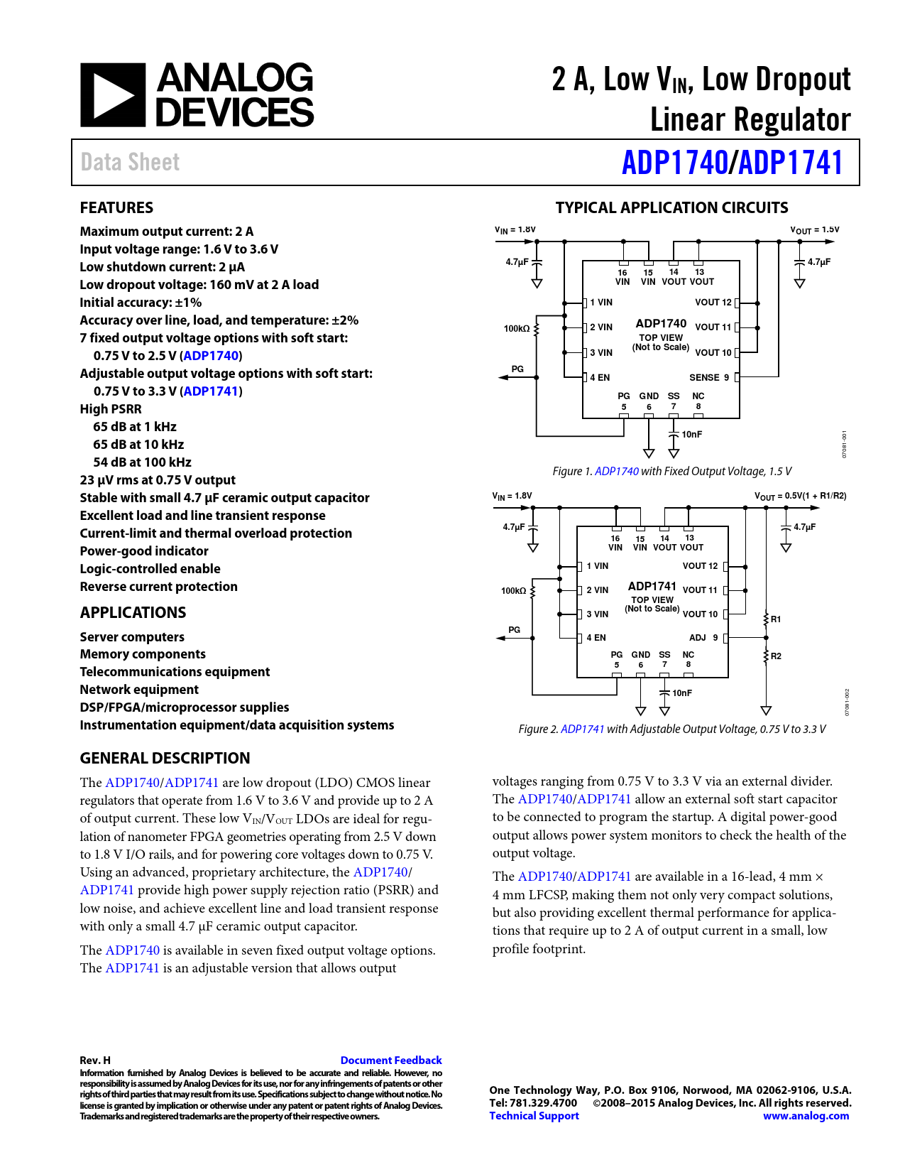
2 A, Low VIN, Low Dropout Linear Regulator Data Sheet ADP1740/ ADP1741 FEATURES TYPICAL APPLICATION CIRCUITS Maximum output current: 2 A VIN = 1.8V VOUT = 1.5V Input voltage range: 1.6 V to 3.6 V Low shutdown current: 2 µA 4.7µF 4.7µF 16 15 14 13 Low dropout voltage: 160 mV at 2 A load VIN VIN VOUT VOUT Initial accuracy: ±1% 1 VIN VOUT 12 Accuracy over line, load, and temperature: ±2% ADP1740 2 VIN 100kΩ VOUT 11 7 fixed output voltage options with soft start: TOP VIEW (Not to Scale) 0.75 V to 2.5 V (ADP1740) 3 VIN VOUT 10 Adjustable output voltage options with soft start: PG 4 EN SENSE 9 0.75 V to 3.3 V (ADP1741) PG GND SS NC High PSRR 5 6 7 8 65 dB at 1 kHz 10nF 65 dB at 10 kHz
001
54 dB at 100 kHz
07081- Figure 1. ADP1740 with Fixed Output Voltage, 1.5 V
23 μV rms at 0.75 V output Stable with small 4.7 µF ceramic output capacitor VIN = 1.8V VOUT = 0.5V(1 + R1/R2) Excellent load and line transient response Current-limit and thermal overload protection 4.7µF 4.7µF 16 15 14 13 Power-good indicator VIN VIN VOUT VOUT Logic-controlled enable 1 VIN VOUT 12 Reverse current protection ADP1741 2 VIN 100kΩ VOUT 11 TOP VIEW APPLICATIONS (Not to Scale) 3 VIN VOUT 10 R1 Server computers PG 4 EN ADJ 9 Memory components PG GND SS NC R2 Telecommunications equipment 5 6 7 8 Network equipment 10nF
002
DSP/FPGA/microprocessor supplies
07081-
Instrumentation equipment/data acquisition systems
Figure 2. ADP1741 with Adjustable Output Voltage, 0.75 V to 3.3 V
GENERAL DESCRIPTION
The ADP1740/ADP1741 are low dropout (LDO) CMOS linear voltages ranging from 0.75 V to 3.3 V via an external divider. regulators that operate from 1.6 V to 3.6 V and provide up to 2 A The ADP1740/ADP1741 al ow an external soft start capacitor of output current. These low VIN/VOUT LDOs are ideal for regu- to be connected to program the startup. A digital power-good lation of nanometer FPGA geometries operating from 2.5 V down output al ows power system monitors to check the health of the to 1.8 V I/O rails, and for powering core voltages down to 0.75 V. output voltage. Using an advanced, proprietary architecture, the ADP1740/ The ADP1740/ADP1741 are available in a 16-lead, 4 mm × ADP1741 provide high power supply rejection ratio (PSRR) and 4 mm LFCSP, making them not only very compact solutions, low noise, and achieve excellent line and load transient response but also providing excel ent thermal performance for applica- with only a small 4.7 µF ceramic output capacitor. tions that require up to 2 A of output current in a small, low The ADP1740 is available in seven fixed output voltage options. profile footprint. The ADP1741 is an adjustable version that al ows output
Rev. H Document Feedback Information furnished by Analog Devices is believed to be accurate and reliable. However, no responsibility is assumed by Analog Devices for its use, nor for any infringements of patents or other rights of third parties that may result from its use. Specifications subject to change without notice. No One Technology Way, P.O. Box 9106, Norwood, MA 02062-9106, U.S.A. license is granted by implication or otherwise under any patent or patent rights of Analog Devices. Tel: 781.329.4700 ©2008–2015 Analog Devices, Inc. All rights reserved. Trademarks and registered trademarks are the property of their respective owners. Technical Support www.analog.com
Document Outline FEATURES APPLICATIONS TYPICAL APPLICATION CIRCUITS GENERAL DESCRIPTION TABLE OF CONTENTS REVISION HISTORY SPECIFICATIONS INPUT AND OUTPUT CAPACITOR, RECOMMENDED SPECIFICATIONS ABSOLUTE MAXIMUM RATINGS THERMAL DATA THERMAL RESISTANCE ESD CAUTION PIN CONFIGURATIONS AND FUNCTION DESCRIPTIONS TYPICAL PERFORMANCE CHARACTERISTICS THEORY OF OPERATION SOFT START FUNCTION ADJUSTABLE OUTPUT VOLTAGE (ADP1741) ENABLE FEATURE POWER-GOOD FEATURE REVERSE CURRENT PROTECTION FEATURE APPLICATIONS INFORMATION CAPACITOR SELECTION Output Capacitor Input Bypass Capacitor Input and Output Capacitor Properties UNDERVOLTAGE LOCKOUT CURRENT-LIMIT AND THERMAL OVERLOAD PROTECTION THERMAL CONSIDERATIONS PCB LAYOUT CONSIDERATIONS OUTLINE DIMENSIONS ORDERING GUIDE

 аккумуляторов")


