Datasheet AD8429 (Analog Devices)
| Производитель | Analog Devices |
| Описание | 1 nV/√Hz Low Noise Instrumentation Amplifier |
| Страниц / Страница | 20 / 1 — 1 nV/√Hz Low Noise. Instrumentation Amplifier. Data Sheet. AD8429. … |
| Версия | A |
| Формат / Размер файла | PDF / 668 Кб |
| Язык документа | английский |
1 nV/√Hz Low Noise. Instrumentation Amplifier. Data Sheet. AD8429. FEATURES. PIN CONNECTION DIAGRAM. Low noise. 1 nV/√Hz input noise
Модельный ряд для этого даташита
Текстовая версия документа
1 nV/√Hz Low Noise Instrumentation Amplifier Data Sheet AD8429 FEATURES PIN CONNECTION DIAGRAM Low noise AD8429 1 nV/√Hz input noise –IN 1 8 +VS 45 nV/√Hz output noise RG 2 7 VOUT High accuracy dc performance (AD8429BRZ) RG 3 6 REF 90 dB CMRR minimum (G = 1) +IN 4 5 –VS
1
50 μV maximum input offset voltage
00
TOP VIEW
0-
(Not to Scale)
73
0.02% maximum gain accuracy (G = 1)
09
Excellent ac specifications
Figure 1.
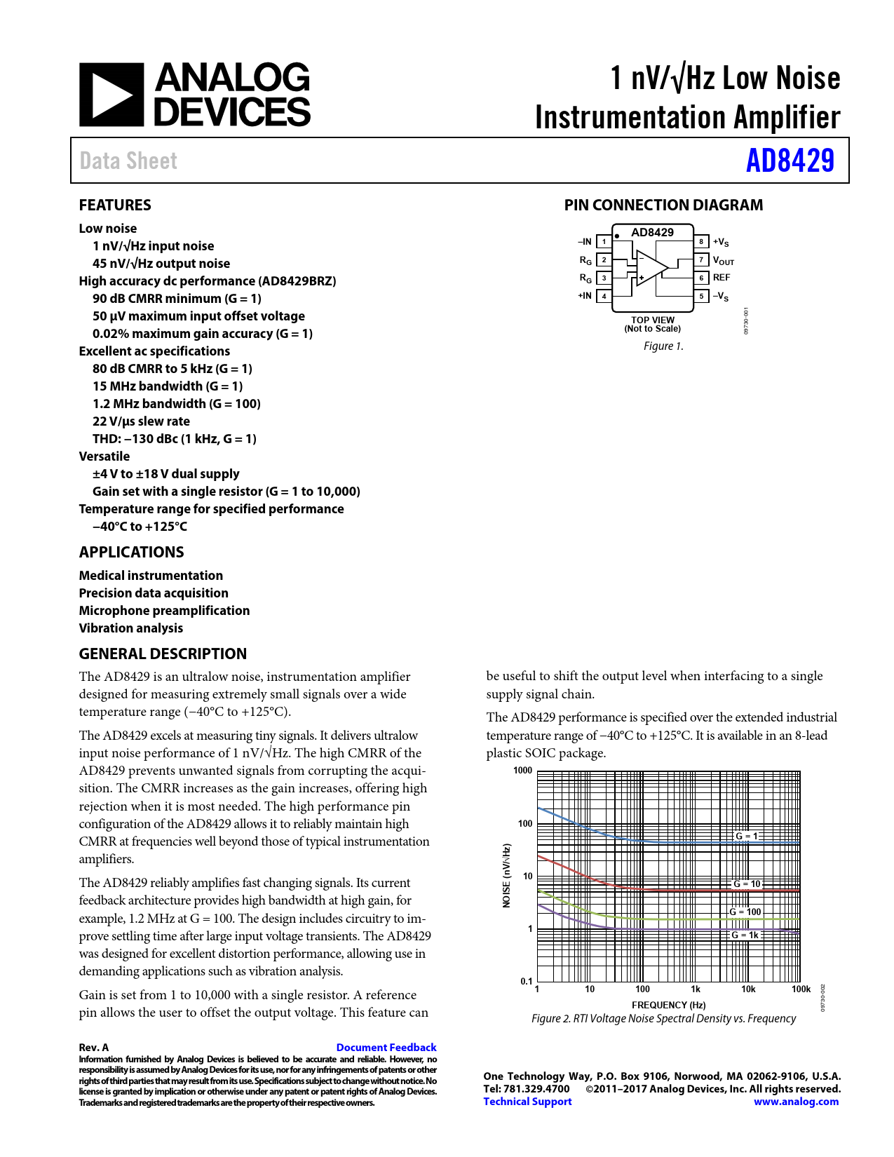
80 dB CMRR to 5 kHz (G = 1) 15 MHz bandwidth (G = 1) 1.2 MHz bandwidth (G = 100) 22 V/μs slew rate THD: −130 dBc (1 kHz, G = 1) Versatile ±4 V to ±18 V dual supply Gain set with a single resistor (G = 1 to 10,000) Temperature range for specified performance −40°C to +125°C APPLICATIONS Medical instrumentation Precision data acquisition Microphone preamplification Vibration analysis GENERAL DESCRIPTION
The AD8429 is an ultralow noise, instrumentation amplifier be useful to shift the output level when interfacing to a single designed for measuring extremely small signals over a wide supply signal chain. temperature range (−40°C to +125°C). The AD8429 performance is specified over the extended industrial The AD8429 excels at measuring tiny signals. It delivers ultralow temperature range of −40°C to +125°C. It is available in an 8-lead input noise performance of 1 nV/√Hz. The high CMRR of the plastic SOIC package. AD8429 prevents unwanted signals from corrupting the acqui-
1000
sition. The CMRR increases as the gain increases, offering high rejection when it is most needed. The high performance pin configuration of the AD8429 allows it to reliably maintain high
100
CMRR at frequencies well beyond those of typical instrumentation
G = 1 )
amplifiers.
√Hz V/ 10
The AD8429 reliably amplifies fast changing signals. Its current
G = 10 ISE (n
feedback architecture provides high bandwidth at high gain, for
O N G = 100
example, 1.2 MHz at G = 100. The design includes circuitry to im-
1
prove settling time after large input voltage transients. The AD8429
G = 1k
was designed for excellent distortion performance, allowing use in demanding applications such as vibration analysis.
0.1 1 10 100 1k 10k 100k
2 Gain is set from 1 to 10,000 with a single resistor. A reference -00
FREQUENCY (Hz)
730 pin allows the user to offset the output voltage. This feature can 09 Figure 2. RTI Voltage Noise Spectral Density vs. Frequency
Rev. A Document Feedback Information furnished by Analog Devices is believed to be accurate and reliable. However, no responsibility is assumed by Analog Devices for its use, nor for any infringements of patents or other rights of third parties that may result from its use. Specifications subject to change without notice. No One Technology Way, P.O. Box 9106, Norwood, MA 02062-9106, U.S.A. license is granted by implication or otherwise under any patent or patent rights of Analog Devices. Tel: 781.329.4700 ©2011–2017 Analog Devices, Inc. All rights reserved. Trademarks and registered trademarks are the property of their respective owners. Technical Support www.analog.com
Document Outline FEATURES APPLICATIONS PIN CONNECTION DIAGRAM GENERAL DESCRIPTION REVISION HISTORY SPECIFICATIONS ABSOLUTE MAXIMUM RATINGS THERMAL RESISTANCE ESD CAUTION PIN CONFIGURATION AND FUNCTION DESCRIPTIONS TYPICAL PERFORMANCE CHARACTERISTICS THEORY OF OPERATION ARCHITECTURE RG Power Dissipation REFERENCE TERMINAL INPUT VOLTAGE RANGE LAYOUT Common-Mode Rejection Ratio over Frequency Power Supplies and Grounding Reference Pin INPUT BIAS CURRENT RETURN PATH INPUT PROTECTION Input Voltages Beyond the Rails Large Differential Input Voltage at High Gain IMAX RADIO FREQUENCY INTERFERENCE (RFI) CALCULATING THE NOISE OF THE INPUT STAGE Source Resistance Noise Voltage Noise of the Instrumentation Amplifier Current Noise of the Instrumentation Amplifier Total Noise Density Calculation OUTLINE DIMENSIONS ORDERING GUIDE

 аккумуляторов")


