DatasheetsDatasheet ADA4950-1/ADA4950-2 (Analog Devices)
Datasheet ADA4950-1/ADA4950-2 (Analog Devices)
| Производитель | Analog Devices |
| Описание | Low Power Selectable Gain Differential ADC Driver, G = 1, 2, 3 |
| Страниц / Страница | 26 / 1 — Low Power, Selectable Gain. Differential ADC Driver, G = 1, 2, 3. Data … |
| Версия | B |
| Формат / Размер файла | PDF / 608 Кб |
| Язык документа | английский |
Low Power, Selectable Gain. Differential ADC Driver, G = 1, 2, 3. Data Sheet. ADA4950-1/. ADA4950-2. FEATURES
Модельный ряд для этого даташита
Текстовая версия документа
Low Power, Selectable Gain Differential ADC Driver, G = 1, 2, 3 Data Sheet ADA4950-1/ ADA4950-2 FEATURES FUNCTIONAL BLOCK DIAGRAMS High performance at low power ADA4950-1 S S S S High speed –V –V –V –V −3 dB bandwidth of 750 MHz, G = 1 16 15 14 13 0.1 dB flatness to 210 MHz, VOUT, dm = 2 V p-p, RL, dm = 200 Ω Slew rate: 2900 V/µs, 25% to 75% +INB 1 12 PD Fast 0.1% settling time of 9 ns +INA 2 11 –OUT –INA 3 10 +OUT Low power: 9.5 mA per amplifier –INB 4 9 V Low harmonic distortion OCM 108 dB SFDR @ 10 MHz 5 6 7 8
001
S S S S 98 dB SFDR @ 20 MHz +V +V +V +V
07957-
Low output voltage noise: 9.2 nV/√Hz, G = 1, RTO
Figure 1. ADA4950-1
±0.2 mV typical input offset voltage ADA4950-2 Selectable differential gains of 1, 2, and 3 1 Differential-to-differential or single-ended-to-differential S1 S1 UT NA1 NB1 I I D1 + + –V –V P –O operation 24 23 22 21 20 19 Adjustable output common-mode voltage –INA1 1 18 Input common-mode range shifted down by 1 V +OUT1 BE –INB1 2 17 VOCM1 Wide supply range: +3 V to ±5 V +V 3 16 S1 –VS2 Available in 16-lead and 24-lead LFCSP packages +V 4 15 S1 –VS2 +INB2 5 14 PD2 APPLICATIONS +INA2 6 13 –OUT2 ADC drivers 7 8 9 Single-ended-to-differential converters 10 11 12 2 S2 S2 T2
002
IF and baseband gain blocks NA2 NB2 CM +V +V –I –I OV OU+
07957-
Differential buffers
Figure 2. ADA4950-2
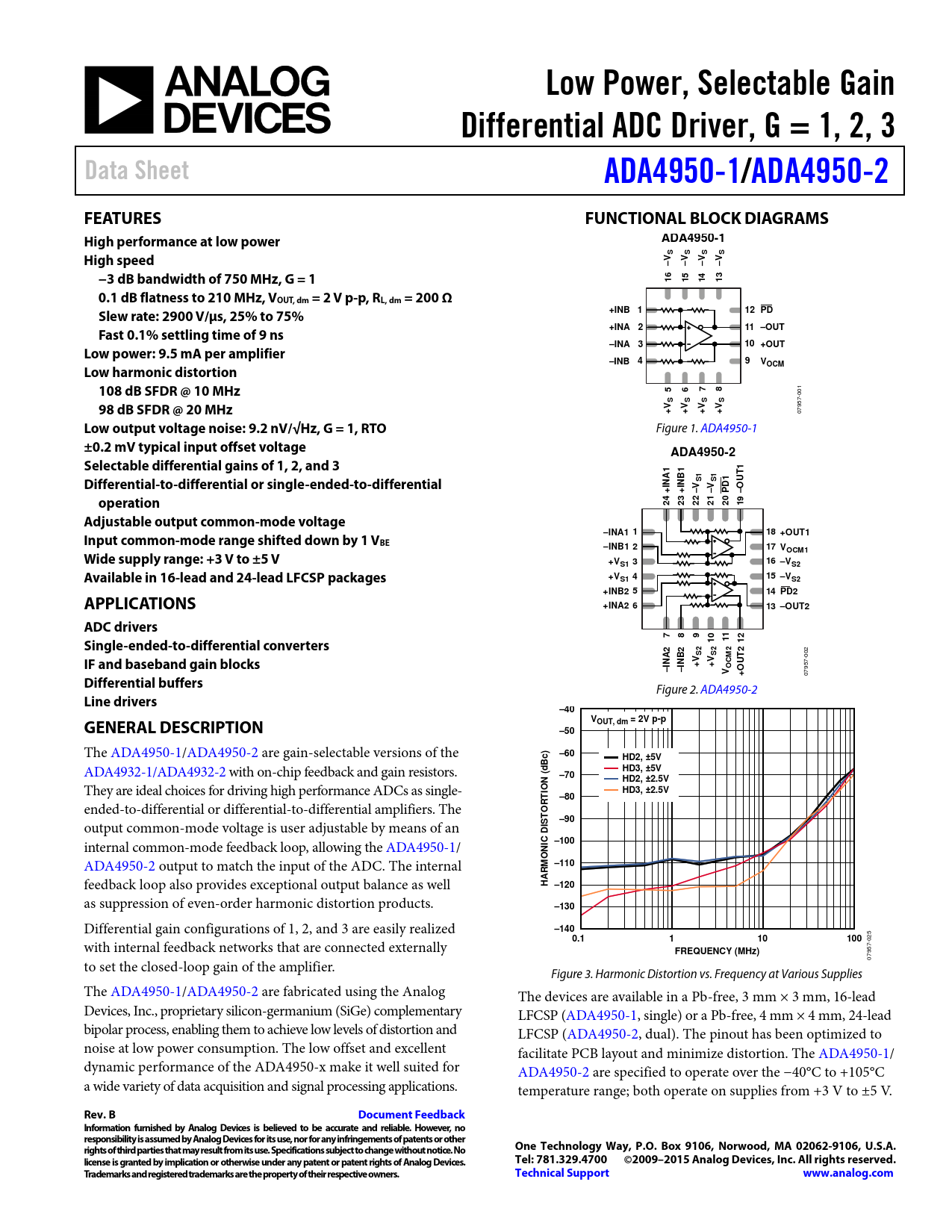
Line drivers –40 GENERAL DESCRIPTION VOUT, dm = 2V p-p –50
The ADA4950-1/ADA4950-2 are gain-selectable versions of the
–60 HD2, ±5V Bc)
ADA4932-1/ADA4932-2 with on-chip feedback and gain resistors.
d HD3, ±5V –70 N ( HD2, ±2.5V
They are ideal choices for driving high performance ADCs as single-
IO HD3, ±2.5V –80
ended-to-differential or differential-to-differential amplifiers. The
RT O T
output common-mode voltage is user adjustable by means of an
–90 S
internal common-mode feedback loop, al owing the ADA4950-1/
C DI –100 NI O
ADA4950-2 output to match the input of the ADC. The internal
–110
feedback loop also provides exceptional output balance as well
HARM –120
as suppression of even-order harmonic distortion products.
–130
Differential gain configurations of 1, 2, and 3 are easily realized
–140
with internal feedback networks that are connected externally
0.1 1 10 100
025
FREQUENCY (MHz)
to set the closed-loop gain of the amplifier. 07957- Figure 3. Harmonic Distortion vs. Frequency at Various Supplies The ADA4950-1/ADA4950-2 are fabricated using the Analog The devices are available in a Pb-free, 3 mm × 3 mm, 16-lead Devices, Inc., proprietary silicon-germanium (SiGe) complementary LFCSP (ADA4950-1, single) or a Pb-free, 4 mm × 4 mm, 24-lead bipolar process, enabling them to achieve low levels of distortion and LFCSP (ADA4950-2, dual). The pinout has been optimized to noise at low power consumption. The low offset and excellent facilitate PCB layout and minimize distortion. The ADA4950-1/ dynamic performance of the ADA4950-x make it wel suited for ADA4950-2 are specified to operate over the −40°C to +105°C a wide variety of data acquisition and signal processing applications. temperature range; both operate on supplies from +3 V to ±5 V.
Rev. B Document Feedback Information furnished by Analog Devices is believed to be accurate and reliable. However, no responsibility is assumed by Analog Devices for its use, nor for any infringements of patents or other rights of third parties that may result from its use. Specifications subject to change without notice. No One Technology Way, P.O. Box 9106, Norwood, MA 02062-9106, U.S.A. license is granted by implication or otherwise under any patent or patent rights of Analog Devices. Tel: 781.329.4700 ©2009–2015 Analog Devices, Inc. All rights reserved. Trademarks and registered trademarks are the property of their respective owners. Technical Support www.analog.com
Document Outline Features Applications General Description Functional Block Diagrams Table of Contents Revision History Specifications ±5 V Operation Differential Inputs to VOUT, dm Performance VOCM to VOUT, cm Performance General Performance 5 V Operation Differential Inputs to VOUT, dm Performance VOCM to VOUT, cm Performance General Performance Absolute Maximum Ratings Thermal Resistance Maximum Power Dissipation ESD Caution Pin Configurations and Function Descriptions Typical Performance Characteristics Test Circuits Terminology Theory of Operation Applications Information Analyzing an Application Circuit Selecting the Closed-Loop Gain Estimating the Output Noise Voltage Calculating the Input Impedance for an Application Circuit Terminating a Single-Ended Input Input Common-Mode Voltage Range Input and Output Capacitive AC Coupling Input Signal Swing Considerations Setting the Output Common-Mode Voltage Layout, Grounding, and Bypassing High Performance ADC Driving Outline Dimensions Ordering Guide

 аккумуляторов")


