Datasheet AD842 (Analog Devices)
| Производитель | Analog Devices |
| Описание | Wideband, High Output Current, Fast Settling Op Amp |
| Страниц / Страница | 16 / 1 — Wideband, High Output Current. Fast Settling Op Amp. Data Sheet. AD842. … |
| Версия | F |
| Формат / Размер файла | PDF / 362 Кб |
| Язык документа | английский |
Wideband, High Output Current. Fast Settling Op Amp. Data Sheet. AD842. FEATURES. CONNECTION DIAGRAMS. AC performance. NIC
13 предложений от 13 поставщиков Операционные усилители Wideband Hi Outpt Crnt Fast Settling |
| 0502128000
Molex | 1.73 ₽ | |
| AD842JRZ-16
Analog Devices | 339 ₽ | |
| AD842JNZ
Analog Devices | по запросу | |
| EP3SE260F1152I4N
Altera | по запросу | |
Модельный ряд для этого даташита
Текстовая версия документа
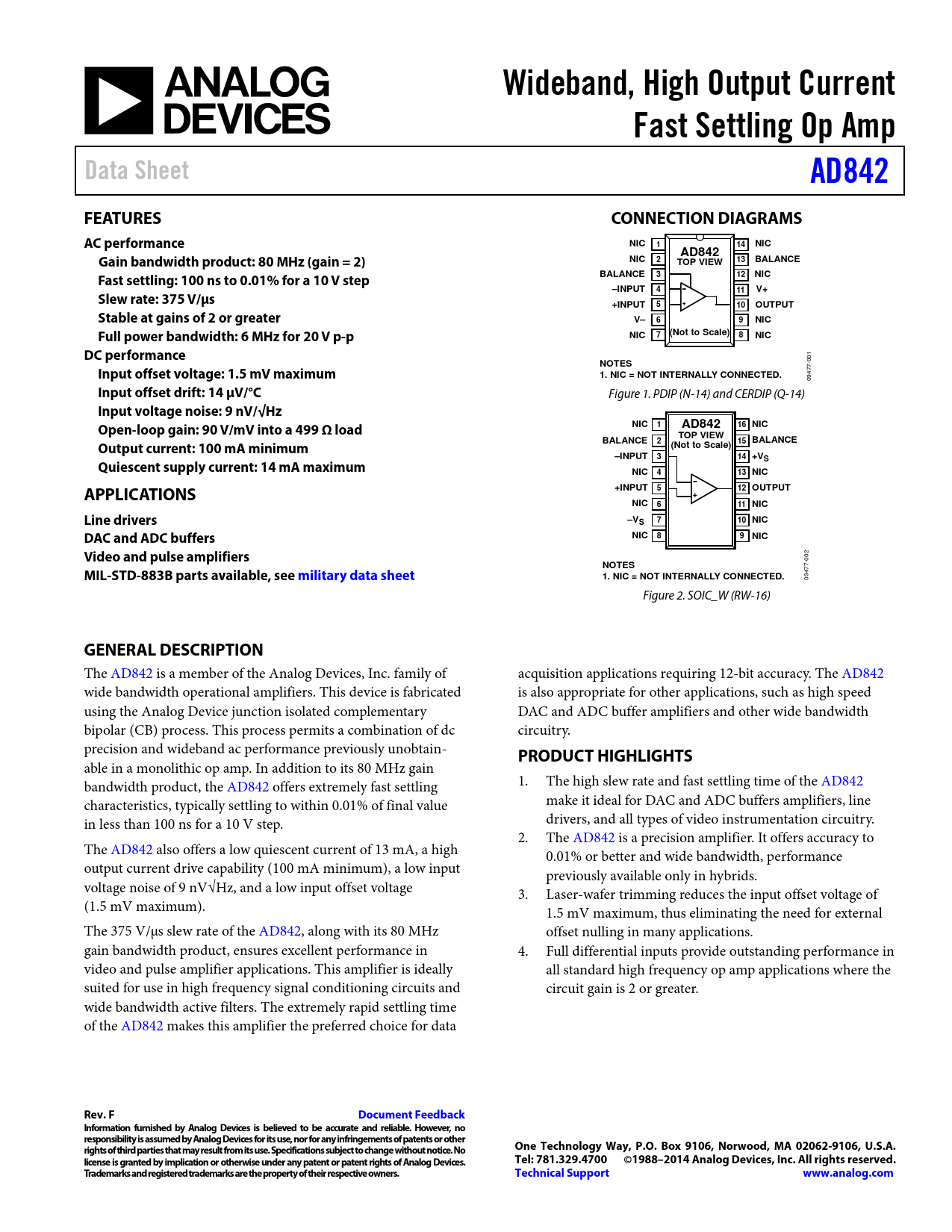
Wideband, High Output Current Fast Settling Op Amp Data Sheet AD842 FEATURES CONNECTION DIAGRAMS AC performance NIC 1 14 NIC AD842 Gain bandwidth product: 80 MHz (gain = 2) NIC 2 13 BALANCE TOP VIEW Fast settling: 100 ns to 0.01% for a 10 V step BALANCE 3 12 NIC –INPUT 4 11 V+ Slew rate: 375 V/µs +INPUT + 5 10 OUTPUT Stable at gains of 2 or greater V– 6 9 NIC Full power bandwidth: 6 MHz for 20 V p-p NIC 7 (Not to Scale) 8 NIC DC performance NOTES
001
Input offset voltage: 1.5 mV maximum 1. NIC = NOT INTERNALLY CONNECTED.
09477-
Input offset drift: 14 µV/°C
Figure 1. PDIP (N-14) and CERDIP (Q-14)
Input voltage noise: 9 nV/√Hz Open-loop gain: 90 V/mV into a 499 Ω load NIC 1 AD842 16 NIC TOP VIEW BALANCE Output current: 100 mA minimum BALANCE 2 15 (Not to Scale) –INPUT 3 14 +V Quiescent supply current: 14 mA maximum S NIC 4 13 NIC APPLICATIONS +INPUT 5 12 OUTPUT + NIC 6 11 NIC Line drivers –V 7 10 S NIC DAC and ADC buffers NIC 8 9 NIC Video and pulse amplifiers
002
NOTES MIL-STD-883B parts available, see military data sheet 1. NIC = NOT INTERNALLY CONNECTED.
09477- Figure 2. SOIC_W (RW-16)
GENERAL DESCRIPTION
The AD842 is a member of the Analog Devices, Inc. family of acquisition applications requiring 12-bit accuracy. The AD842 wide bandwidth operational amplifiers. This device is fabricated is also appropriate for other applications, such as high speed using the Analog Device junction isolated complementary DAC and ADC buffer amplifiers and other wide bandwidth bipolar (CB) process. This process permits a combination of dc circuitry. precision and wideband ac performance previously unobtain-
PRODUCT HIGHLIGHTS
able in a monolithic op amp. In addition to its 80 MHz gain bandwidth product, the AD842 offers extremely fast settling 1. The high slew rate and fast settling time of the AD842 characteristics, typically settling to within 0.01% of final value make it ideal for DAC and ADC buffers amplifiers, line in less than 100 ns for a 10 V step. drivers, and al types of video instrumentation circuitry. 2. The AD842 is a precision amplifier. It offers accuracy to The AD842 also offers a low quiescent current of 13 mA, a high 0.01% or better and wide bandwidth, performance output current drive capability (100 mA minimum), a low input previously available only in hybrids. voltage noise of 9 nV√Hz, and a low input offset voltage 3. Laser-wafer trimming reduces the input offset voltage of (1.5 mV maximum). 1.5 mV maximum, thus eliminating the need for external The 375 V/µs slew rate of the AD842, along with its 80 MHz offset nulling in many applications. gain bandwidth product, ensures excellent performance in 4. Full differential inputs provide outstanding performance in video and pulse amplifier applications. This amplifier is ideally al standard high frequency op amp applications where the suited for use in high frequency signal conditioning circuits and circuit gain is 2 or greater. wide bandwidth active filters. The extremely rapid settling time of the AD842 makes this amplifier the preferred choice for data
Rev. F Document Feedback Information furnished by Analog Devices is believed to be accurate and reliable. However, no responsibility is assumed by Analog Devices for its use, nor for any infringements of patents or other rights of third parties that may result from its use. Specifications subject to change without notice. No One Technology Way, P.O. Box 9106, Norwood, MA 02062-9106, U.S.A. license is granted by implication or otherwise under any patent or patent rights of Analog Devices. Tel: 781.329.4700 ©1988–2014 Analog Devices, Inc. All rights reserved. Trademarks and registered trademarks are the property of their respective owners. Technical Support www.analog.com
Document Outline Features Applications Connection Diagrams General Description Product Highlights Table of Contents Revision History Specifications Electrical Characteristics—±15 V Operation Absolute Maximum Ratings Thermal Characteristics ESD Caution Metalization Photograph Typical Performance Characteristics Theory of Operation Offset Nulling Settling Time Grounding and Bypassing Capacitive Load Driving Ability Using a Heat Sink Terminated Line Driver Overdrive Recovery Outline Dimensions Ordering Guide

 аккумуляторов")


