Datasheet CD4013B (Texas Instruments)
| Производитель | Texas Instruments |
| Описание | CMOS Dual D-Type Flip-Flop |
| Страниц / Страница | 28 / 1 — CD4013B. CD4013B CMOS Dual D-Type Flip-Flop. 1 Features. 3 Description. 2 … |
| Версия | E |
| Формат / Размер файла | PDF / 1.6 Мб |
| Язык документа | английский |
CD4013B. CD4013B CMOS Dual D-Type Flip-Flop. 1 Features. 3 Description. 2 Applications. Device Information(1). PART NUMBER. PACKAGE
Текстовая версия документа
link to page 1 Product Sample & Technical Tools & Support & Folder Buy Documents Software Community
CD4013B
SCHS023E – NOVEMBER 1998 – REVISED SEPTEMBER 2016
CD4013B CMOS Dual D-Type Flip-Flop 1 Features 3 Description
• Asynchronous Set-Reset Capability The CD4013B device consists of two identical, 1 independent data-type flip-flops. Each flip-flop has • Static Flip-Flop Operation independent data, set, reset, and clock inputs and Q • Medium-Speed Operation: 16 MHz (Typical) Clock and Q outputs. These devices can be used for shift Toggle Rate at 10-V Supply register applications, and, by connecting Q output to • Standardized Symmetrical Output Characteristics the data input, for counter and toggle applications. The logic level present at the D input is transferred to • Maximum Input Current Of 1-µA at 18 V Over Full the Q output during the positive-going transition of the Package Temperature Range: clock pulse. Setting or resetting is independent of the – 100 nA at 18 V and 25°C clock and is accomplished by a high level on the set • Noise Margin (Over Full Package Temperature or reset line, respectively. Range): The CD4013B types are supplied in 14-pin dual-in- – 1 V at V line plastic packages (E suffix), 14-pin small-outline DD = 5 V – 2 V at V packages (M, MT, M96, and NSR suffixes), and DD = 10 V 14-pin thin shrink small-outline packages (PW and – 2.5 V at VDD = 15 V PWR suffixes).
2 Applications Device Information(1)
• Power Delivery
PART NUMBER PACKAGE BODY SIZE (NOM)
• Grid Infrastructure CD4013BE PDIP (14) 19.30 mm x 6.35 mm • Medical, Healthcare, and Fitness CD4013BF CDIP (14) 19.50 mm x 6.92 mm • Body Electronics and Lighting CD4013BM SOIC (14) 8.65 mm x 3.90 mm CD4013BNS SO (14) 10.20 mm x 5.30 mm • Building Automation CD4013BPW TSSOP (14) 5.00 mm x 4.40 mm • Telecom Infrastructure (1) For all available packages, see the orderable addendum at • Test and Measurement the end of the data sheet.
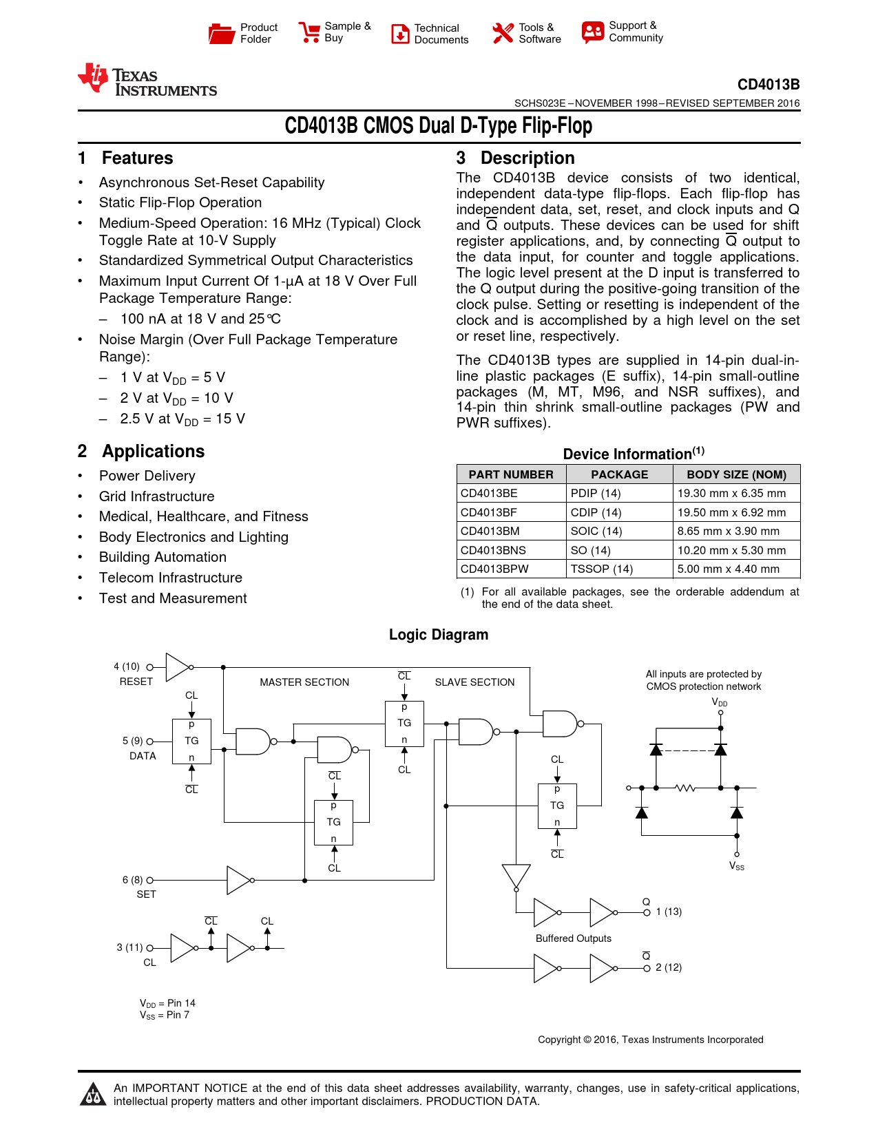
Logic Diagram
4 (10) CL All inputs are protected by RESET MASTER SECTION SLAVE SECTION CMOS protection network CL VDD p p TG 5 (9) TG n DATA n CL CL CL CL p p TG TG n n CL V CL SS 6 (8) SET Q 1 (13) CL CL Buffered Outputs 3 (11) Q CL 2 (12) VDD = Pin 14 VSS = Pin 7 Copyright © 2016, Texas Instruments Incorporated 1 An IMPORTANT NOTICE at the end of this data sheet addresses availability, warranty, changes, use in safety-critical applications, intellectual property matters and other important disclaimers. PRODUCTION DATA. Document Outline 1 Features 2 Applications 3 Description Table of Contents 4 Revision History 5 Pin Configuration and Functions 6 Specifications 6.1 Absolute Maximum Ratings 6.2 ESD Ratings 6.3 Recommended Operating Conditions 6.4 Thermal Information 6.5 Electrical Characteristics: Static 6.6 Electrical Characteristics: Dynamic 6.7 Typical Characteristics 7 Detailed Description 7.1 Overview 7.2 Functional Block Diagram 7.3 Feature Description 7.4 Device Functional Modes 8 Application and Implementation 8.1 Application Information 8.2 Typical Application 8.2.1 Design Requirements 8.2.2 Detailed Design Procedure 8.2.3 Application Curve 9 Power Supply Recommendations 10 Layout 10.1 Layout Guidelines 10.2 Layout Example 11 Device and Documentation Support 11.1 Documentation Support 11.1.1 Related Documentation 11.2 Receiving Notification of Documentation Updates 11.3 Community Resources 11.4 Trademarks 11.5 Electrostatic Discharge Caution 11.6 Glossary 12 Mechanical, Packaging, and Orderable Information

 аккумуляторов")


