Datasheet ADA4941-1 (Analog Devices)
| Производитель | Analog Devices |
| Описание | Single-Supply, Differential 18-Bit ADC Driver |
| Страниц / Страница | 24 / 1 — Single-Supply, Differential,. 18-Bit ADC Driver. Data Sheet. ADA4941-1. … |
| Версия | D |
| Формат / Размер файла | PDF / 859 Кб |
| Язык документа | английский |
Single-Supply, Differential,. 18-Bit ADC Driver. Data Sheet. ADA4941-1. FEATURES. FUNCTIONAL BLOCK DIAGRAM
Модельный ряд для этого даташита
Текстовая версия документа
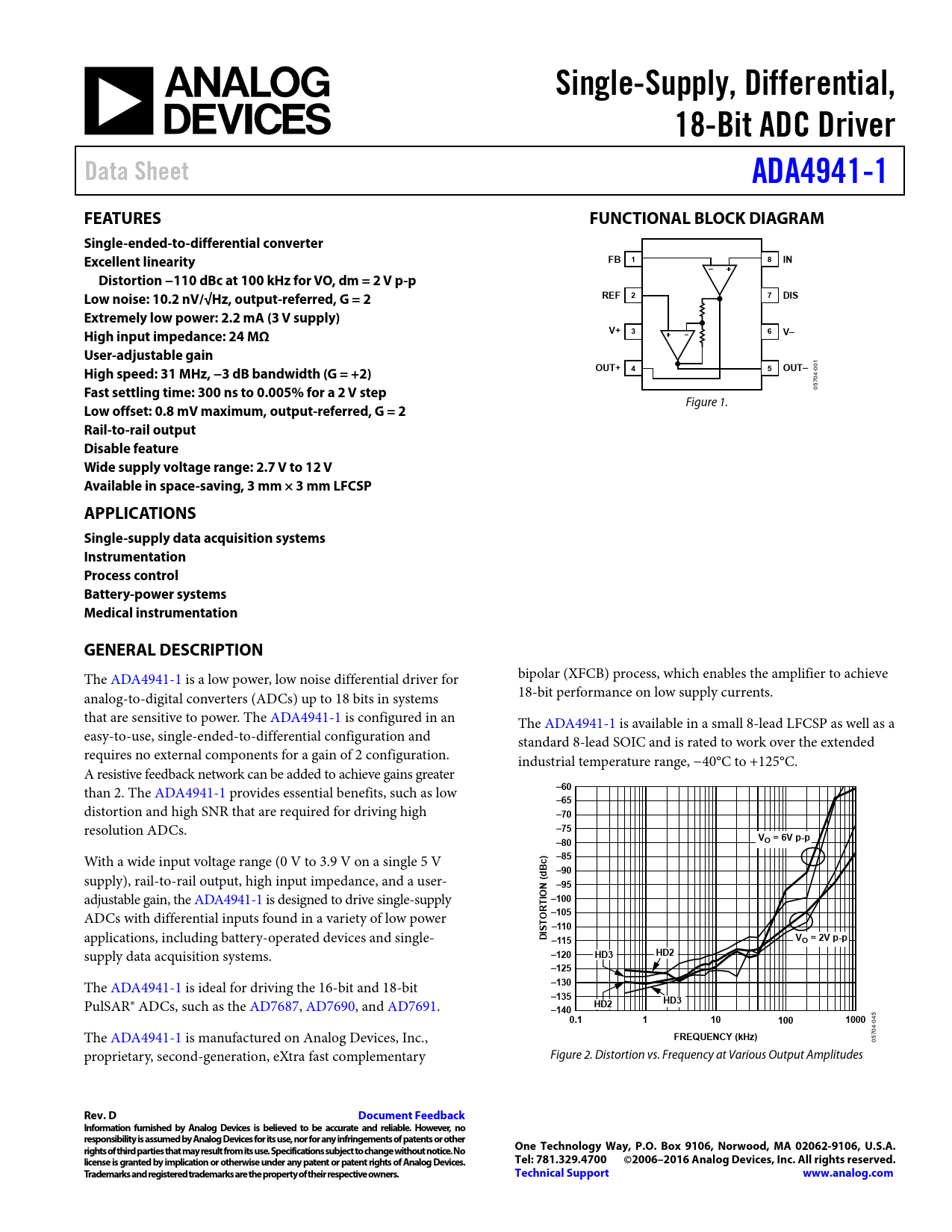
Single-Supply, Differential, 18-Bit ADC Driver Data Sheet ADA4941-1 FEATURES FUNCTIONAL BLOCK DIAGRAM Single-ended-to-differential converter Excellent linearity FB 1 8 IN Distortion −110 dBc at 100 kHz for VO, dm = 2 V p-p Low noise: 10.2 nV/√Hz, output-referred, G = 2 REF 2 7 DIS Extremely low power: 2.2 mA (3 V supply) V+ 3 6 High input impedance: 24 MΩ V– User-adjustable gain OUT+ 4 5 OUT–
010
High speed: 31 MHz, −3 dB bandwidth (G = +2)
4- 570
Fast settling time: 300 ns to 0.005% for a 2 V step
0 Figure 1.
Low offset: 0.8 mV maximum, output-referred, G = 2 Rail-to-rail output Disable feature Wide supply voltage range: 2.7 V to 12 V Available in space-saving, 3 mm × 3 mm LFCSP APPLICATIONS Single-supply data acquisition systems Instrumentation Process control Battery-power systems Medical instrumentation GENERAL DESCRIPTION
The ADA4941-1 is a low power, low noise differential driver for bipolar (XFCB) process, which enables the amplifier to achieve analog-to-digital converters (ADCs) up to 18 bits in systems 18-bit performance on low supply currents. that are sensitive to power. The ADA4941-1 is configured in an The ADA4941-1 is available in a small 8-lead LFCSP as well as a easy-to-use, single-ended-to-differential configuration and standard 8-lead SOIC and is rated to work over the extended requires no external components for a gain of 2 configuration. industrial temperature range, −40°C to +125°C. A resistive feedback network can be added to achieve gains greater
–60
than 2. The ADA4941-1 provides essential benefits, such as low
–65
distortion and high SNR that are required for driving high
–70
resolution ADCs.
–75 VO = 6V p-p –80
With a wide input voltage range (0 V to 3.9 V on a single 5 V
–85 Bc) d –90
supply), rail-to-rail output, high input impedance, and a user-
( N –95
adjustable gain, the ADA4941-1 is designed to drive single-supply
IO T –100 R –105
ADCs with differential inputs found in a variety of low power
O T S –110
applications, including battery-operated devices and single-
DI V –115 O = 2V p-p
supply data acquisition systems.
–120 HD3 HD2 –125
The ADA4941-1 is ideal for driving the 16-bit and 18-bit
–130 –135
PulSAR® ADCs, such as the AD7687, AD7690, and AD7691.
HD2 HD3 –140
5
0.1 1 10 100 1000
044- The ADA4941-1 is manufactured on Analog Devices, Inc.,
FREQUENCY (kHz)
70 05 proprietary, second-generation, eXtra fast complementary Figure 2. Distortion vs. Frequency at Various Output Amplitudes
Rev. D Document Feedback Information furnished by Analog Devices is believed to be accurate and reliable. However, no responsibility is assumed by Analog Devices for its use, nor for any infringements of patents or other rights of third parties that may result from its use. Specifications subject to change without notice. No One Technology Way, P.O. Box 9106, Norwood, MA 02062-9106, U.S.A. license is granted by implication or otherwise under any patent or patent rights of Analog Devices. Tel: 781.329.4700 ©2006–2016 Analog Devices, Inc. All rights reserved. Trademarks and registered trademarks are the property of their respective owners. Technical Support www.analog.com
Document Outline FEATURES APPLICATIONS FUNCTIONAL BLOCK DIAGRAM GENERAL DESCRIPTION TABLE OF CONTENTS REVISION HISTORY SPECIFICATIONS ABSOLUTE MAXIMUM RATINGS THERMAL RESISTANCE MAXIMUM POWER DISSIPATION ESD CAUTION PIN CONFIGURATION AND FUNCTION DESCRIPTIONS TYPICAL PERFORMANCE CHARACTERISTICS THEORY OF OPERATION BASIC OPERATION DC ERROR CALCULATIONS OUTPUT VOLTAGE NOISE FREQUENCY RESPONSE VS. CLOSED-LOOP GAIN APPLICATIONS INFORMATION OVERVIEW USING THE REF PIN INTERNAL FEEDBACK NETWORK POWER DISSIPATION DISABLE FEATURE ADDING A 3-POLE, SALLEN-KEY FILTER DRIVING THE AD7687 ADC GAIN OF −2 CONFIGURATION OUTLINE DIMENSIONS ORDERING GUIDE

 аккумуляторов")


