
Datasheet Texas Instruments SN74LVC1G332 — Даташит
| Производитель | Texas Instruments |
| Серия | SN74LVC1G332 |
Single 3-Input Positive-OR Gate
Datasheets
SN74LVC1G332 datasheet
PDF, 1.4 Мб, Версия: E, Файл опубликован: 11 янв 2012
Выписка из документа
Цены
 Купить SN74LVC1G332 на РадиоЛоцман.Цены — от 3.07 до 43 ₽ Купить SN74LVC1G332 на РадиоЛоцман.Цены — от 3.07 до 43 ₽49 предложений от 26 поставщиков Логический элемент ИЛИ, семейство LVC, 3 входа, 50мА, 1.65В до 5.5В, SOT-23-6 | |||
| SN74LVC1G332DBVR Texas Instruments | 3.07 ₽ | ||
| SN74LVC1G332DBVR Texas Instruments | 3.13 ₽ | ||
| SN74LVC1G332DCKR Texas Instruments | от 14 ₽ | ||
| SN74LVC1G332DBVR | 16 ₽ | ||
 аккумуляторов")

Статус
| 74LVC1G332DBVRG4 | 74LVC1G332DCKRE4 | SN74LVC1G332DBVR | SN74LVC1G332DCKR | SN74LVC1G332DCKRG4 | SN74LVC1G332DRLR | SN74LVC1G332DRY2 | SN74LVC1G332DRYR | SN74LVC1G332DSF2 | SN74LVC1G332DSFR | SN74LVC1G332YZPR | |
|---|---|---|---|---|---|---|---|---|---|---|---|
| Статус продукта | В производстве | В производстве | В производстве | В производстве | В производстве | В производстве | В производстве | В производстве | В производстве | В производстве | В производстве |
| Доступность образцов у производителя | Нет | Да | Да | Да | Нет | Да | Да | Нет | Да | Да | Да |
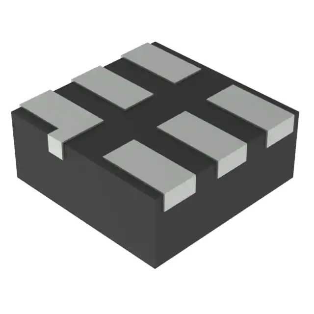
Корпус / Упаковка / Маркировка
| 74LVC1G332DBVRG4 | 74LVC1G332DCKRE4 | SN74LVC1G332DBVR | SN74LVC1G332DCKR | SN74LVC1G332DCKRG4 | SN74LVC1G332DRLR | SN74LVC1G332DRY2 | SN74LVC1G332DRYR | SN74LVC1G332DSF2 | SN74LVC1G332DSFR | SN74LVC1G332YZPR | |
|---|---|---|---|---|---|---|---|---|---|---|---|
| N | 1 | 2 | 3 | 4 | 5 | 6 | 7 | 8 | 9 | 10 | 11 |
| Pin | 6 | 6 | 6 | 6 | 6 | 6 | 6 | 6 | 6 | 6 | 6 |
| Package Type | DBV | DCK | DBV | DCK | DCK | DRL | DRY | DRY | DSF | DSF | YZP |
| Industry STD Term | SOT-23 | SOT-SC70 | SOT-23 | SOT-SC70 | SOT-SC70 | SOT-5X3 | USON | USON | X2SON | X2SON | DSBGA |
| JEDEC Code | R-PDSO-G | R-PDSO-G | R-PDSO-G | R-PDSO-G | R-PDSO-G | R-PDSO-N | R-PDSO-N | R-PDSO-N | S-PDSO-N | S-PDSO-N | R-XBGA-N |
| Package QTY | 3000 | 3000 | 3000 | 3000 | 3000 | 4000 | 5000 | 5000 | 5000 | 5000 | 3000 |
| Carrier | LARGE T&R | LARGE T&R | LARGE T&R | LARGE T&R | LARGE T&R | LARGE T&R | LARGE T&R | LARGE T&R | LARGE T&R | LARGE T&R | LARGE T&R |
| Маркировка | C2CF | CZK | C2CF | CZR | CZF | CZR | CZ | CZ | CZ | CZ | CZN |
| Width (мм) | 1.6 | 1.25 | 1.6 | 1.25 | 1.25 | 1.2 | 1 | 1 | 1 | 1 | .9 |
| Length (мм) | 2.9 | 2 | 2.9 | 2 | 2 | 1.6 | 1.45 | 1.45 | 1 | 1 | 1.5 |
| Thickness (мм) | 1.2 | .9 | 1.2 | .9 | .9 | .55 | .5 | .5 | .35 | .35 | 2 |
| Pitch (мм) | .95 | .65 | .95 | .65 | .65 | .5 | .5 | .5 | .35 | .35 | .5 |
| Max Height (мм) | 1.45 | 1.1 | 1.45 | 1.1 | 1.1 | .6 | .6 | .6 | .4 | .4 | .5 |
| Mechanical Data | Скачать | Скачать | Скачать | Скачать | Скачать | Скачать | Скачать | Скачать | Скачать | Скачать | Скачать |
Параметры
| Parameters / Models | 74LVC1G332DBVRG4 | 74LVC1G332DCKRE4 | SN74LVC1G332DBVR | SN74LVC1G332DCKR | SN74LVC1G332DCKRG4 | SN74LVC1G332DRLR | SN74LVC1G332DRY2 | SN74LVC1G332DRYR | SN74LVC1G332DSF2 | SN74LVC1G332DSFR | SN74LVC1G332YZPR |
|---|---|---|---|---|---|---|---|---|---|---|---|
| 3-State Output | No | No | No | No | No | No | No | No | No | No | No |
| Bits | 1 | 1 | 1 | 1 | 1 | 1 | 1 | 1 | 1 | 1 | 1 |
| F @ Nom Voltage(Max), Mhz | 150 | 150 | 150 | 150 | 150 | 150 | 150 | 150 | 150 | 150 | 150 |
| Gate Type | OR | OR | OR | OR | OR | OR | OR | OR | OR | OR | OR |
| ICC @ Nom Voltage(Max), мА | 0.01 | 0.01 | 0.01 | 0.01 | 0.01 | 0.01 | 0.01 | 0.01 | 0.01 | 0.01 | 0.01 |
| Logic | True | True | True | True | True | True | True | True | True | True | True |
| Рабочий диапазон температур, C | от -40 до 125,-40 до 85 | от -40 до 125,-40 до 85 | от -40 до 125,-40 до 85 | от -40 до 125,-40 до 85 | от -40 до 125,-40 до 85 | от -40 до 125,-40 до 85 | от -40 до 125,-40 до 85 | от -40 до 125,-40 до 85 | от -40 до 125,-40 до 85 | от -40 до 125,-40 до 85 | от -40 до 125,-40 до 85 |
| Output Drive (IOL/IOH)(Max), мА | 32/-32 | 32/-32 | 32/-32 | 32/-32 | 32/-32 | 32/-32 | 32/-32 | 32/-32 | 32/-32 | 32/-32 | 32/-32 |
| Package Group | SOT-23 | SC70 | SOT-23 | SC70 | SC70 | SOT-5X3 | SON | SON | SON | SON | DSBGA |
| Package Size: mm2:W x L, PKG | 6SOT-23: 8 mm2: 2.8 x 2.9(SOT-23) | 6SC70: 4 mm2: 2.1 x 2(SC70) | 6SOT-23: 8 mm2: 2.8 x 2.9(SOT-23) | 6SC70: 4 mm2: 2.1 x 2(SC70) | 6SC70: 4 mm2: 2.1 x 2(SC70) | 6SOT-5X3: 3 mm2: 1.6 x 1.6(SOT-5X3) | See datasheet (SON) | See datasheet (SON) | See datasheet (SON) | See datasheet (SON) | See datasheet (DSBGA) |
| Rating | Catalog | Catalog | Catalog | Catalog | Catalog | Catalog | Catalog | Catalog | Catalog | Catalog | Catalog |
| Schmitt Trigger | No | No | No | No | No | No | No | No | No | No | No |
| Special Features | Ioff,down translation to Vcc,low power | Ioff,down translation to Vcc,low power | Ioff,down translation to Vcc,low power | Ioff,down translation to Vcc,low power | Ioff,down translation to Vcc,low power | Ioff,down translation to Vcc,low power | Ioff,down translation to Vcc,low power | Ioff,down translation to Vcc,low power | Ioff,down translation to Vcc,low power | Ioff,down translation to Vcc,low power | Ioff,down translation to Vcc,low power |
| Sub-Family | OR Gate | OR Gate | OR Gate | OR Gate | OR Gate | OR Gate | OR Gate | OR Gate | OR Gate | OR Gate | OR Gate |
| Technology Family | LVC | LVC | LVC | LVC | LVC | LVC | LVC | LVC | LVC | LVC | LVC |
| VCC(Max), В | 5.5 | 5.5 | 5.5 | 5.5 | 5.5 | 5.5 | 5.5 | 5.5 | 5.5 | 5.5 | 5.5 |
| VCC(Min), В | 1.65 | 1.65 | 1.65 | 1.65 | 1.65 | 1.65 | 1.65 | 1.65 | 1.65 | 1.65 | 1.65 |
| Voltage(Nom), В | 1.8,2.5,3.3,5 | 1.8,2.5,3.3,5 | 1.8,2.5,3.3,5 | 1.8,2.5,3.3,5 | 1.8,2.5,3.3,5 | 1.8,2.5,3.3,5 | 1.8,2.5,3.3,5 | 1.8,2.5,3.3,5 | 1.8,2.5,3.3,5 | 1.8,2.5,3.3,5 | 1.8,2.5,3.3,5 |
| tpd @ Nom Voltage(Max), нс | 17.2,6.2,4.8,3.5 | 17.2,6.2,4.8,3.5 | 17.2,6.2,4.8,3.5 | 17.2,6.2,4.8,3.5 | 17.2,6.2,4.8,3.5 | 17.2,6.2,4.8,3.5 | 17.2,6.2,4.8,3.5 | 17.2,6.2,4.8,3.5 | 17.2,6.2,4.8,3.5 | 17.2,6.2,4.8,3.5 | 17.2,6.2,4.8,3.5 |
Экологический статус
| 74LVC1G332DBVRG4 | 74LVC1G332DCKRE4 | SN74LVC1G332DBVR | SN74LVC1G332DCKR | SN74LVC1G332DCKRG4 | SN74LVC1G332DRLR | SN74LVC1G332DRY2 | SN74LVC1G332DRYR | SN74LVC1G332DSF2 | SN74LVC1G332DSFR | SN74LVC1G332YZPR | |
|---|---|---|---|---|---|---|---|---|---|---|---|
| RoHS | Совместим | Совместим | Совместим | Совместим | Совместим | Совместим | Совместим | Совместим | Совместим | Совместим | Совместим |
Application Notes
- LVC Characterization InformationPDF, 114 Кб, Файл опубликован: 1 дек 1996
This document provides characterization information about low-voltage logic (LVL) that operates from a 3.3-V power supply. It addresses the issues of interfacing to 5-V logic ac performance power considerations input and output characteristics and signal integrity for this family of devices. - Use of the CMOS Unbuffered Inverter in Oscillator CircuitsPDF, 796 Кб, Файл опубликован: 6 ноя 2003
CMOS devices have a high input impedance high gain and high bandwidth. These characteristics are similar to ideal amplifier characteristics and hence a CMOS buffer or inverter can be used in an oscillator circuit in conjunction with other passive components. Now CMOS oscillator circuits are widely used in high-speed applications because they are economical easy to use and take significantly - 16-Bit Widebus Logic Families in 56-Ball 0.65-mm Pitch Very Thin Fine-Pitch BGA (Rev. B)PDF, 895 Кб, Версия: B, Файл опубликован: 22 май 2002
TI?s 56-ball MicroStar Jr.E package registered under JEDEC MO-225 has demonstrated through modeling and experimentation that it is an optimal solution for reducing inductance and capacitance improving thermal performance and minimizing board area usage in integrated bus functions. Multiple functions released in the 56-ball MicroStar Jr.E package have superior performance characteristics compa - Bus-Interface Devices With Output-Damping Resistors Or Reduced-Drive Outputs (Rev. A)PDF, 105 Кб, Версия: A, Файл опубликован: 1 авг 1997
The spectrum of bus-interface devices with damping resistors or balanced/light output drive currently offered by various logic vendors is confusing at best. Inconsistencies in naming conventions and methods used for implementation make it difficult to identify the best solution for a given application. This report attempts to clarify the issue by looking at several vendors? approaches and discussi - Understanding Advanced Bus-Interface Products Design GuidePDF, 253 Кб, Файл опубликован: 1 май 1996
- Power-Up 3-State (PU3S) Circuits in TI Standard Logic DevicesPDF, 209 Кб, Файл опубликован: 10 май 2002
Many telecom and networking applications require that cards be inserted and extracted from a live backplane without interrupting data or damaging components. To achieve this interface terminals of the card must be electrically isolated from the bus system during insertion or extraction from the backplane. To facilitate this Texas Instruments provides bus-interface and logic devices with features - How to Select Little Logic (Rev. A)PDF, 1.1 Мб, Версия: A, Файл опубликован: 26 июл 2016
TI Little Logic devices are logic-gate devices assembled in a small single- dual- or triple- gate package. Little Logic devices are widely used in portable equipment such as mobile phones MP3 players and notebook computers. Little Logic devices also are used in desktop computers and telecommunications. Little Logic gates are common components for easy PC board routing schematic design and b - Migration From 3.3-V To 2.5-V Power Supplies For Logic DevicesPDF, 115 Кб, Файл опубликован: 1 дек 1997
This application report explores the possibilities for migrating to 3.3-V and 2.5-V power supplies and discusses the implications.Customers are successfully using a wide range of low-voltage 3.3-V logic devices. These devices are within Texas Instruments (TI) advanced low-voltage CMOS (ALVC) crossbar technology (CBT) crossbar technology with integrated diode (CBTD) low-voltage crossbar techn - Texas Instruments Little Logic Application ReportPDF, 359 Кб, Файл опубликован: 1 ноя 2002
Portable and consumer electronic systems? needs present greater challenges today than ever before. Engineers strive to design smaller faster lower-cost systems to meet the market demand. Consequently the semiconductor industry faces a growing need to increase operating speed minimize power consumption and reduce packaging size. Texas Instruments manufactures a variety of Little Logic semicond - Selecting the Right Level Translation Solution (Rev. A)PDF, 313 Кб, Версия: A, Файл опубликован: 22 июн 2004
Supply voltages continue to migrate to lower nodes to support today's low-power high-performance applications. While some devices are capable of running at lower supply nodes others might not have this capability. To haveswitching compatibility between these devices the output of each driver must be compliant with the input of the receiver that it is driving. There are several level-translati - Live InsertionPDF, 150 Кб, Файл опубликован: 1 окт 1996
Many applications require the ability to exchange modules in electronic systems without removing the supply voltage from the module (live insertion). For example an electronic telephone exchange must always remain operational even during module maintenance and repair. To avoid damaging components additional circuitry modifications are necessary. This document describes in detail the phenomena tha - Implications of Slow or Floating CMOS Inputs (Rev. D)PDF, 260 Кб, Версия: D, Файл опубликован: 23 июн 2016
- CMOS Power Consumption and CPD Calculation (Rev. B)PDF, 89 Кб, Версия: B, Файл опубликован: 1 июн 1997
Reduction of power consumption makes a device more reliable. The need for devices that consume a minimum amount of power was a major driving force behind the development of CMOS technologies. As a result CMOS devices are best known for low power consumption. However for minimizing the power requirements of a board or a system simply knowing that CMOS devices may use less power than equivale - Input and Output Characteristics of Digital Integrated CircuitsPDF, 1.7 Мб, Файл опубликован: 1 окт 1996
This report contains a comprehensive collection of the input and output characteristic curves of typical integrated circuits from various logic families. These curves go beyond the information given in data sheets by providing additional details regarding the characteristics of the components. This knowledge is particularly useful when for example a decision must be made as to which circuit shou - Selecting the Right Texas Instruments Signal SwitchPDF, 769 Кб, Файл опубликован: 7 сен 2001
Texas Instruments offers a wide variety of electronic switches (digital analog bilateral bilateral analog) in a variety of families including CBT CBTLV HC LV and LVC. Depending on the application the right solution may be an analog switch that passes digital signals or vice versa. This application report summarizes the various switching technologies and provides considerations for choosi
Модельный ряд
Серия: SN74LVC1G332 (11)
Классификация производителя
- Semiconductors> Logic> Little Logic

