Datasheet MCP4725 (Microchip) - 38
| Производитель | Microchip |
| Описание | 12-Bit Digital-to-Analog Converter with EEPROM Memory in SOT-23-6 |
| Страниц / Страница | 50 / 38 — MCP4725 |
| Формат / Размер файла | PDF / 1.5 Мб |
| Язык документа | английский |
MCP4725
Модельный ряд для этого даташита
Текстовая версия документа
link to page 37
MCP4725
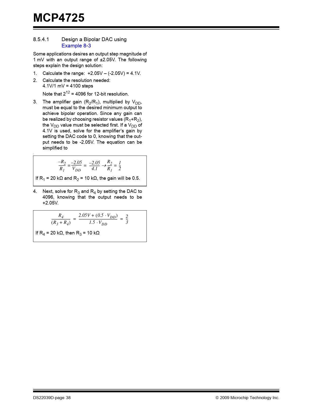
8.5.4.1 Design a Bipolar DAC using Example 8-3 Some applications desires an output step magnitude of 1 mV with an output range of ±2.05V. The following steps explain the design solution: 1. Calculate the range: +2.05V – (-2.05V) = 4.1V. 2. Calculate the resolution needed: 4.1V/1 mV = 4100 steps Note that 212 = 4096 for 12-bit resolution. 3. The amplifier gain (R2/R1), multiplied by VDD, must be equal to the desired minimum output to achieve bipolar operation. Since any gain can be realized by choosing resistor values (R1+R2), the VDD value must be selected first. If a VDD of 4.1V is used, solve for the amplifier’s gain by setting the DAC code to 0, knowing that the out- put needs to be -2.05V. The equation can be simplified to : –R R 2 –2.05 – 1 ----- =------- 2.05 = ------- 2 → --- = - R V 4.1 R 2 1 DD 1 If R1 = 20 kΩ and R2 = 10 kΩ, the gain will be 0.5. 4. Next, solve for R3 and R4 by setting the DAC to 4096, knowing that the output needs to be +2.05V. R 2.05V + (0.5 ⋅ V ) 4 DD 2 (------------ = ------------------------- = - R + R ) 1.5 ⋅ V 3 3 4 DD If R4 = 20 kΩ, then R3 = 10 kΩ DS22039D-page 38 © 2009 Microchip Technology Inc. Document Outline 1.0 Electrical Characteristics 2.0 Typical Performance Curves FIGURE 2-1: DNL vs. Code (VDD = 5.5V). FIGURE 2-2: DNL vs. Code and Temperature (TA = -40°C to +125°C). FIGURE 2-3: DNL vs. Code (VDD = 2.7V). FIGURE 2-4: DNL vs. Code and Temperature (TA = -40°C to +125°C). FIGURE 2-5: INL vs. Code. FIGURE 2-6: INL vs. Code and Temperature (VDD = 5.5V). FIGURE 2-7: INL vs. Code and Temperature (VDD = 2.7V). FIGURE 2-8: Zero Scale Error vs. Temperature (Code = 000d). FIGURE 2-9: Full Scale Error vs. Temperature (Code = 4095d). FIGURE 2-10: Output Error vs. Temperature (Code = 4000d). FIGURE 2-11: IDD vs. Temperature. FIGURE 2-12: IDD Histogram . FIGURE 2-13: IDD Histogram. FIGURE 2-14: Offset Error vs. Temperature and VDD. FIGURE 2-15: VOUT vs. Resistive Load. FIGURE 2-16: Source and Sink Current Capability. FIGURE 2-17: VIN High Threshold vs. Temperature and VDD. FIGURE 2-18: VIN Low Threshold vs. Temperature and VDD. FIGURE 2-19: Full Scale Settling Time. FIGURE 2-20: Full Scale Settling Time. FIGURE 2-21: Half Scale Settling Time. FIGURE 2-22: Half Scale Settling Time. FIGURE 2-23: Code Change Glitch. FIGURE 2-24: Exiting Power Down Mode. 3.0 Pin Descriptions TABLE 3-1: Pin Function Table 3.1 Analog Output Voltage (VOUT) 3.2 Supply Voltage (VDD or VSS) 3.3 Serial Data Pin (SDA) 3.4 Serial Clock Pin (SCL) 3.5 Device Address Selection Pin (A0) 4.0 Terminology 4.1 Resolution 4.2 LSB 4.3 Integral Nonlinearity (INL) or Relative Accuracy FIGURE 4-1: INL Accuracy. 4.4 Differential Nonlinearity (DNL) FIGURE 4-2: DNL Accuracy. 4.5 Offset Error FIGURE 4-3: Offset Error. 4.6 Gain Error 4.7 Full Scale Error (FSE) FIGURE 4-4: Gain Error and Full Scale Error. 4.8 Gain Error Drift 4.9 Offset Error Drift 4.10 Settling Time 4.11 Major-Code Transition Glitch 4.12 Digital Feedthrough 5.0 General Description 5.1 Output Voltage 5.2 LSB SIZE TABLE 5-1: LSB SIZES for MCP4725 (example) 5.3 Voltage Reference 5.4 Reset Conditions 5.5 Normal and Power-Down Modes TABLE 5-2: Power-down bits FIGURE 5-1: Output Stage for Power- Down Mode. 5.6 Non-Volatile EEPROM Memory TABLE 5-3: EEPROM Memory and Factory Default Settings (Total number of bits: 14 bits) TABLE 5-4: DAC register 6.0 Theory Of Operation 6.1 Write Commands TABLE 6-1: Input Data Coding TABLE 6-2: Write Command Type FIGURE 6-1: Fast Mode Write Command. FIGURE 6-2: Write Commands for DAC Input Register and EEPROM. 6.2 read command FIGURE 6-3: Read Command and Output Data Format. 7.0 I2C Serial Interface Communication 7.1 OVERVIEW 7.2 Device Addressing FIGURE 7-1: Device Addressing. 7.3 General Call FIGURE 7-2: General Call Address Format. 7.4 High-Speed (HS) Mode 7.5 I2C BUS CHARACTERISTICS FIGURE 7-3: Data Transfer Sequence On The Serial Bus. TABLE 7-1: I2c serial timing Specifications FIGURE 7-4: I2C Bus Timing Data. 8.0 Typical Applications 8.1 Connecting to I2C BUS using Pull-Up Resistors FIGURE 8-1: I2C Bus Interface Connection with A0 pin tied to VSS. FIGURE 8-2: I2C Bus Connection Test. 8.2 Using Non-Volatile EEPROM Memory 8.3 Power Supply Considerations 8.4 Layout Considerations 8.5 Application Examples FIGURE 8-3: Digitally Controllable Current Source. 9.0 Development Support 9.1 Evaluation & Demonstration Boards FIGURE 9-1: MCP4725 SOT-23-6 Evaluation Board. FIGURE 9-2: Setup for the MCP4725 SOT-23-6 Evaluation Board with PICkit™ Serial Analyzer. FIGURE 9-3: Example of PICkit™ Serial User Interface. 10.0 Packaging Information 10.1 Package Marking Information Corporate Office Atlanta Boston Chicago Cleveland Fax: 216-447-0643 Dallas Detroit Kokomo Toronto Fax: 852-2401-3431 Australia - Sydney China - Beijing China - Shanghai India - Bangalore Korea - Daegu Korea - Seoul Singapore Taiwan - Taipei Fax: 43-7242-2244-393 Denmark - Copenhagen France - Paris Germany - Munich Italy - Milan Spain - Madrid UK - Wokingham Worldwide Sales and Service


 Купить MCP4725A0T-E/MAY на РадиоЛоцман.Цены
