Datasheet ADSP-BF531, ADSP-BF532, ADSP-BF533 (Analog Devices) - 56
| Производитель | Analog Devices |
| Описание | Blackfin Embedded Processor |
| Страниц / Страница | 64 / 56 — ADSP-BF531/. ADSP-BF532. /ADSP-BF533. 176-LEAD LQFP PINOUT. Table 45. … |
| Версия | I |
| Формат / Размер файла | PDF / 2.5 Мб |
| Язык документа | английский |
ADSP-BF531/. ADSP-BF532. /ADSP-BF533. 176-LEAD LQFP PINOUT. Table 45. 176-Lead LQFP Pin Assignment (Alphabetical by Signal)
Модельный ряд для этого даташита
Текстовая версия документа
link to page 56 link to page 57
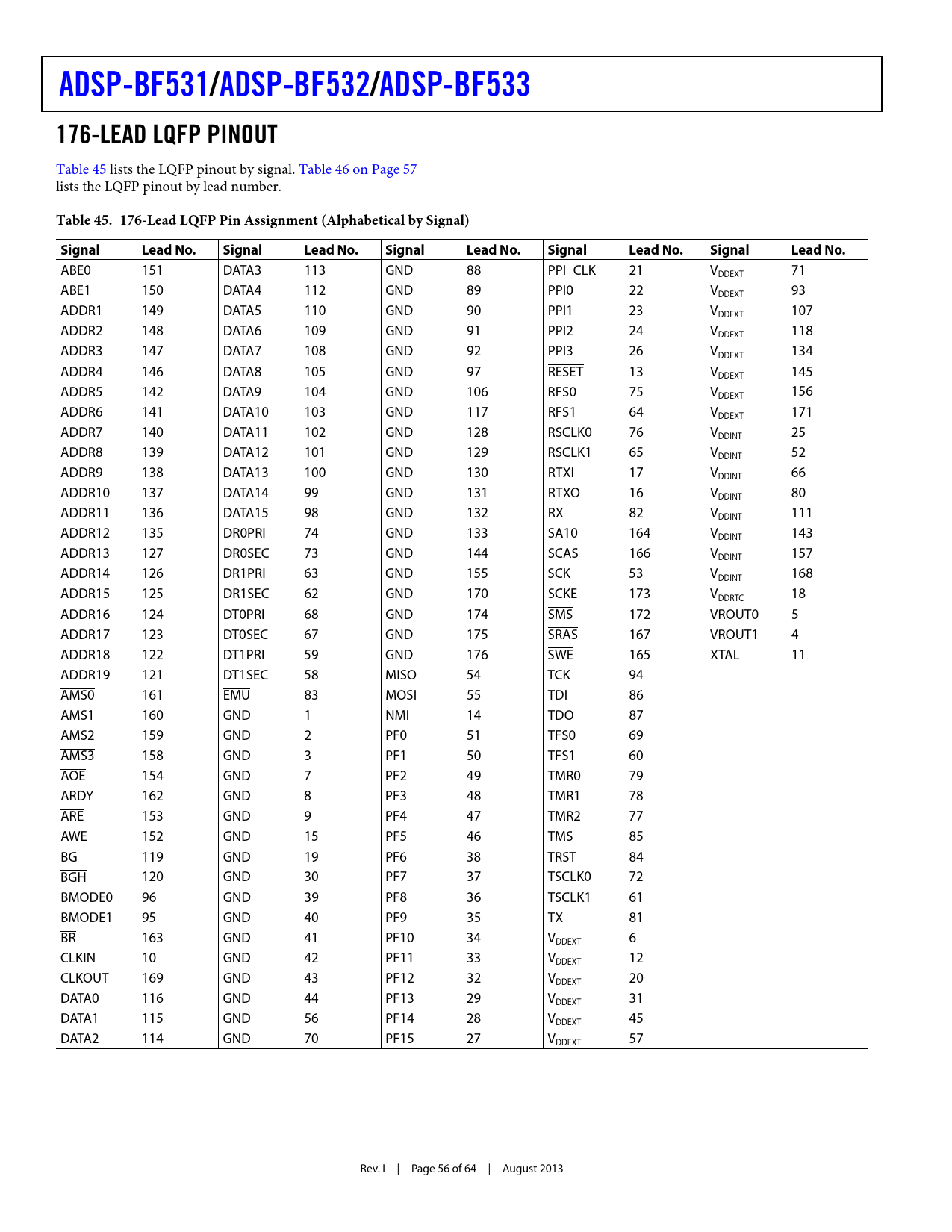
ADSP-BF531/ ADSP-BF532 /ADSP-BF533 176-LEAD LQFP PINOUT
Table 45 lists the LQFP pinout by signal. Table 46 on Page 57 lists the LQFP pinout by lead number.
Table 45. 176-Lead LQFP Pin Assignment (Alphabetical by Signal) Signal Lead No. Signal Lead No. Signal Lead No. Signal Lead No. Signal Lead No.
ABE0 151 DATA3 113 GND 88 PPI_CLK 21 VDDEXT 71 ABE1 150 DATA4 112 GND 89 PPI0 22 VDDEXT 93 ADDR1 149 DATA5 110 GND 90 PPI1 23 VDDEXT 107 ADDR2 148 DATA6 109 GND 91 PPI2 24 VDDEXT 118 ADDR3 147 DATA7 108 GND 92 PPI3 26 VDDEXT 134 ADDR4 146 DATA8 105 GND 97 RESET 13 VDDEXT 145 ADDR5 142 DATA9 104 GND 106 RFS0 75 VDDEXT 156 ADDR6 141 DATA10 103 GND 117 RFS1 64 VDDEXT 171 ADDR7 140 DATA11 102 GND 128 RSCLK0 76 VDDINT 25 ADDR8 139 DATA12 101 GND 129 RSCLK1 65 VDDINT 52 ADDR9 138 DATA13 100 GND 130 RTXI 17 VDDINT 66 ADDR10 137 DATA14 99 GND 131 RTXO 16 VDDINT 80 ADDR11 136 DATA15 98 GND 132 RX 82 VDDINT 111 ADDR12 135 DR0PRI 74 GND 133 SA10 164 VDDINT 143 ADDR13 127 DR0SEC 73 GND 144 SCAS 166 VDDINT 157 ADDR14 126 DR1PRI 63 GND 155 SCK 53 VDDINT 168 ADDR15 125 DR1SEC 62 GND 170 SCKE 173 VDDRTC 18 ADDR16 124 DT0PRI 68 GND 174 SMS 172 VROUT0 5 ADDR17 123 DT0SEC 67 GND 175 SRAS 167 VROUT1 4 ADDR18 122 DT1PRI 59 GND 176 SWE 165 XTAL 11 ADDR19 121 DT1SEC 58 MISO 54 TCK 94 AMS0 161 EMU 83 MOSI 55 TDI 86 AMS1 160 GND 1 NMI 14 TDO 87 AMS2 159 GND 2 PF0 51 TFS0 69 AMS3 158 GND 3 PF1 50 TFS1 60 AOE 154 GND 7 PF2 49 TMR0 79 ARDY 162 GND 8 PF3 48 TMR1 78 ARE 153 GND 9 PF4 47 TMR2 77 AWE 152 GND 15 PF5 46 TMS 85 BG 119 GND 19 PF6 38 TRST 84 BGH 120 GND 30 PF7 37 TSCLK0 72 BMODE0 96 GND 39 PF8 36 TSCLK1 61 BMODE1 95 GND 40 PF9 35 TX 81 BR 163 GND 41 PF10 34 VDDEXT 6 CLKIN 10 GND 42 PF11 33 VDDEXT 12 CLKOUT 169 GND 43 PF12 32 VDDEXT 20 DATA0 116 GND 44 PF13 29 VDDEXT 31 DATA1 115 GND 56 PF14 28 VDDEXT 45 DATA2 114 GND 70 PF15 27 VDDEXT 57 Rev. I | Page 56 of 64 | August 2013 Document Outline Blackfin Embedded Processor Features Memory Peripherals Table Of Contents Revision History General Description Portable Low Power Architecture System Integration Processor Peripherals Blackfin Processor Core Memory Architecture Internal (On-Chip) Memory External (Off-Chip) Memory I/O Memory Space Booting Event Handling Core Event Controller (CEC) System Interrupt Controller (SIC) Event Control DMA Controllers Real-Time Clock Watchdog Timer Timers Serial Ports (SPORTs) Serial Peripheral Interface (SPI) Port UART Port General-Purpose I/O Port F Parallel Peripheral Interface General-Purpose Mode Descriptions Input Mode Frame Capture Mode Output Mode ITU-R 656 Mode Descriptions Active Video Only Mode Vertical Blanking Interval Mode Entire Field Mode Dynamic Power Management Full-On Operating Mode—Maximum Performance Active Operating Mode—Moderate Power Savings Sleep Operating Mode—High Dynamic Power Savings Deep Sleep Operating Mode—Maximum Dynamic Power Savings Hibernate State—Maximum Static Power Savings Power Savings Voltage Regulation Voltage Regulator Layout Guidelines Clock Signals Booting Modes Instruction Set Description Development Tools Integrated Development Environments (IDEs) EZ-KIT Lite Evaluation Board EZ-KIT Lite Evaluation Kits Software Add-Ins for CrossCore Embedded Studio Board Support Packages for Evaluation Hardware Middleware Packages Algorithmic Modules Designing an Emulator-Compatible DSP Board (Target) Additional Information Related Signal Chains Pin Descriptions Specifications Operating Conditions Electrical Characteristics Absolute Maximum Ratings ESD Sensitivity Package Information Timing Specifications Clock and Reset Timing Asynchronous Memory Read Cycle Timing Asynchronous Memory Write Cycle Timing SDRAM Interface Timing External Port Bus Request and Grant Cycle Timing Parallel Peripheral Interface Timing Serial Port Timing Serial Peripheral Interface (SPI) Port—Master Timing Serial Peripheral Interface (SPI) Port—Slave Timing General-Purpose I/O Port F Pin Cycle Timing Universal Asynchronous Receiver-Transmitter (UART) Ports—Receive and Transmit Timing Timer Clock Timing Timer Cycle Timing JTAG Test and Emulation Port Timing Output Drive Currents Test Conditions Output Enable Time Measurement Output Disable Time Measurement Example System Hold Time Calculation Capacitive Loading Thermal Characteristics 160-Ball CSP_BGA Ball Assignment 169-Ball PBGA Ball Assignment 176-Lead LQFP Pinout Outline Dimensions Surface-Mount Design Automotive Products Ordering Guide

 Купить ADSP-BF533SBBZ500 на РадиоЛоцман.Цены — от 1 325 до 19 336 ₽


