Datasheet MPSA05, MPSA06, MPSA55, MPSA56 (ON Semiconductor)
| Производитель | ON Semiconductor |
| Описание | NPN Bipolar Small Signal Transistor |
| Страниц / Страница | 7 / 1 — *Preferred Devices. Voltage and Current are Negative for PNP Transistors. … |
| Версия | 3 |
| Формат / Размер файла | PDF / 92 Кб |
| Язык документа | английский |
*Preferred Devices. Voltage and Current are Negative for PNP Transistors. http://onsemi.com. Features. NPN. PNP. MAXIMUM RATINGS
18 предложений от 14 поставщиков Двухполюсный плоскостной транзистор, TO-92 NPN 80V 0.5A |
| MPS-A06RLRA
| по запросу | |
| MPSA06RLRA
ON Semiconductor | по запросу | |
| MPSA06RLRA
ON Semiconductor | по запросу | |
| MPSA06RLRA
ON Semiconductor | по запросу | |
Модельный ряд для этого даташита
Текстовая версия документа
link to page 1 link to page 6 NPN − MPSA05, MPSA06*; PNP − MPSA55, MPSA56*
*Preferred Devices
Amplifier Transistors
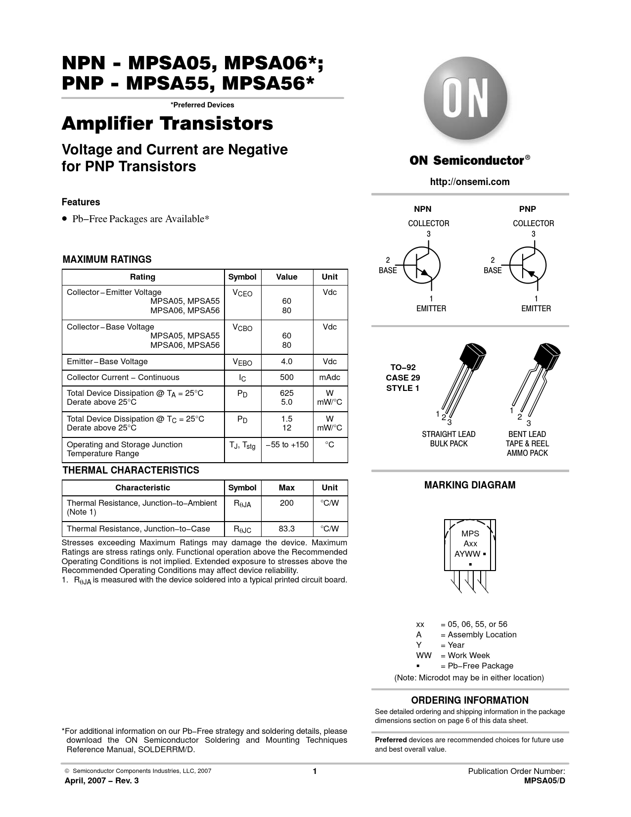
Voltage and Current are Negative for PNP Transistors http://onsemi.com Features NPN PNP
• Pb−Free Packages are Available* COLLECTOR COLLECTOR 3 3
MAXIMUM RATINGS
2 2 BASE BASE
Rating Symbol Value Unit
Collector − Emitter Voltage VCEO Vdc MPSA05, MPSA55 60 1 1 MPSA06, MPSA56 80 EMITTER EMITTER Collector − Base Voltage VCBO Vdc MPSA05, MPSA55 60 MPSA06, MPSA56 80 Emitter − Base Voltage VEBO 4.0 Vdc
TO−92
Collector Current − Continuous IC 500 mAdc
CASE 29 STYLE 1
Total Device Dissipation @ TA = 25°C PD 625 W Derate above 25°C 5.0 mW/°C 1 1 Total Device Dissipation @ T 2 2 C = 25°C PD 1.5 W 3 3 Derate above 25°C 12 mW/°C STRAIGHT LEAD BENT LEAD Operating and Storage Junction TJ, Tstg −55 to +150 °C BULK PACK TAPE & REEL Temperature Range AMMO PACK
THERMAL CHARACTERISTICS Characteristic Symbol Max Unit MARKING DIAGRAM
Thermal Resistance, Junction−to−Ambient RqJA 200 °C/W (Note 1) Thermal Resistance, Junction−to−Case RqJC 83.3 °C/W MPS Stresses exceeding Maximum Ratings may damage the device. Maximum Axx Ratings are stress ratings only. Functional operation above the Recommended AYWW G Operating Conditions is not implied. Extended exposure to stresses above the G Recommended Operating Conditions may affect device reliability. 1. RqJA is measured with the device soldered into a typical printed circuit board. xx = 05, 06, 55, or 56 A = Assembly Location Y = Year WW = Work Week G = Pb−Free Package (Note: Microdot may be in either location)
ORDERING INFORMATION
See detailed ordering and shipping information in the package dimensions section on page 6 of this data sheet. *For additional information on our Pb−Free strategy and soldering details, please download the ON Semiconductor Soldering and Mounting Techniques
Preferred
devices are recommended choices for future use Reference Manual, SOLDERRM/D. and best overall value. © Semiconductor Components Industries, LLC, 2007
1
Publication Order Number:
April, 2007 − Rev. 3 MPSA05/D

 Купить MPSA06RLRA на РадиоЛоцман.Цены — от 2.29 до 51 ₽

