Datasheet 5X2503 (IDT) - 25
| Производитель | IDT |
| Описание | MicroClock Programmable Clock Generator with Embedded Crystal |
| Страниц / Страница | 30 / 25 — SMBus Table Byte 30: OE and DFC Control. Byte 1Eh. Name. Control … |
| Версия | 20171218 |
| Формат / Размер файла | PDF / 418 Кб |
| Язык документа | английский |
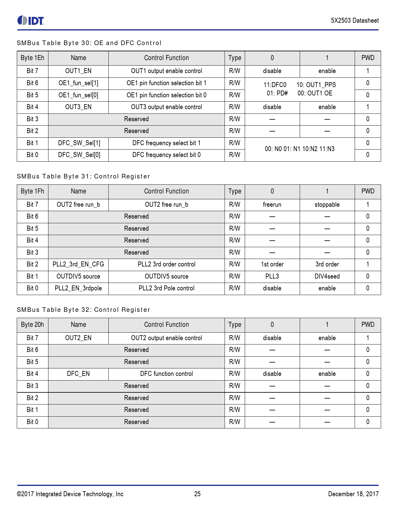
SMBus Table Byte 30: OE and DFC Control. Byte 1Eh. Name. Control Function. Type. PWD. SMBus Table Byte 31: Control Register. Byte 1Fh
Модельный ряд для этого даташита
Текстовая версия документа
5X2503 Datasheet
SMBus Table Byte 30: OE and DFC Control Byte 1Eh Name Control Function Type 0 1 PWD
Bit 7 OUT1_EN OUT1 output enable control R/W disable enable 1 Bit 6 OE1_fun_sel[1] OE1 pin function selection bit 1 R/W 11:DFC0 10: OUT1_PPS 0 01: PD# 00: OUT1 OE Bit 5 OE1_fun_sel[0] OE1 pin function selection bit 0 R/W 0 Bit 4 OUT3_EN OUT3 output enable control R/W disable enable 1 Bit 3 Reserved R/W — — 0 Bit 2 Reserved R/W — — 0 Bit 1 DFC_SW_Sel[1] DFC frequency select bit 1 R/W 0 00: N0 01: N1 10:N2 11:N3 Bit 0 DFC_SW_Sel[0] DFC frequency select bit 0 R/W 0
SMBus Table Byte 31: Control Register Byte 1Fh Name Control Function Type 0 1 PWD
Bit 7 OUT2 free run_b OUT2 free run_b R/W freerun stoppable 1 Bit 6 Reserved R/W — — 0 Bit 5 Reserved R/W — — 0 Bit 4 Reserved R/W — — 0 Bit 3 Reserved R/W — — 0 Bit 2 PLL2_3rd_EN_CFG PLL2 3rd order control R/W 1st order 3rd order 1 Bit 1 OUTDIV5 source OUTDIV5 source R/W PLL3 DIV4seed 0 Bit 0 PLL2_EN_3rdpole PLL2 3rd Pole control R/W disable enable 0
SMBus Table Byte 32: Control Register Byte 20h Name Control Function Type 0 1 PWD
Bit 7 OUT2_EN OUT2 output enable control R/W disable enable 1 Bit 6 Reserved R/W — — 0 Bit 5 Reserved R/W — — 0 Bit 4 DFC_EN DFC function control R/W disable enable 0 Bit 3 Reserved R/W — — 0 Bit 2 Reserved R/W — — 0 Bit 1 Reserved R/W — — 0 Bit 0 Reserved R/W — — 0 ©2017 Integrated Device Technology, Inc 25 December 18, 2017 Document Outline Description Typical Applications Features Output Features Key Specifications Block Diagram Power Group Output Source Selection Register Setting Tables Pin Assignments Figure 1. Pin Assignments for 2.5 × 2.5 mm 12-DFN Package Pin Descriptions Table 1. Pin Descriptions Device Feature and Function DFC – Dynamic Frequency Control Figure 2. DFC Function Block Diagram Table 2. DFC Function Priority DFC Function Programming PPS – Proactive Power Saving Function Figure 3. PPS Function Block Diagram Figure 4. PPS Assertion/Deassertion Timing Chart PPS Function Programming Input Pin Function Table 3. OE1 Pin Function Table Table 4. SDA/SCL Function Selection Spread Spectrum ORT – VCO Overshoot Reduction Technology PLL Features and Descriptions Table 5. Output Divider 1 Table 6. Output Divider 2, 3, and 5 Table 7. Output Divider 4 Output Clock Test Conditions Figure 5. LVCMOS Output Clock Test Condition Absolute Maximum Ratings Table 8. Absolute Maximum Ratings Recommended Operating Conditions Table 9. Recommended Operating Conditions Input Capacitance, LVCMOS Output Impedance, and Internal Pull-down Resistance (TA = +25 °C) Table 10. Input Capacitance, LVCMOS Output Impedance, and Internal Pull-down Resistance Integrated Crystal Characteristics Table 11. Crystal Characteristics DC Electrical Characteristics Table 12. DC Electrical Characteristics 1,2 Electrical Characteristics–Input Parameters Table 13. Electrical Characteristics–Input Parameters 1 DC Electrical Characteristics for 1.8V LVCMOS Table 14. DC Electrical Characteristics – 1.8V LVCMOS AC Electrical Characteristics Table 15. AC Timing Electrical Characteristics – 32.768kHz Table 16. AC Timing Electrical Characteristics – 1.8V Table 17. AC Timing Electrical Characteristics, 1.2V / 1.8V I2C Bus DC Characteristics Table 18. I2C Bus DC Characteristics Table 19. I2C Bus AC Characteristics Spread Spectrum Generation Specifications Table 20. Spread Spectrum Generation Specifications General SMBus Serial Interface Information Package Outline Drawings Figure 6. NDG12 Package Drawing – page 1 Figure 7. NDG12 Package Drawing – page 2 Ordering Information Marking Diagram Revision History

 Купить 5X2503-000NDGI8 на РадиоЛоцман.Цены — от 54 до 590 ₽


