Datasheet ADP5071 (Analog Devices) - 27
| Производитель | Analog Devices |
| Описание | 2 A/1.2 A DC-to-DC Switching Regulator with Independent Positive and Negative Outputs |
| Страниц / Страница | 27 / 27 — Data Sheet. ADP5071. OUTLINE DIMENSIONS. DETAIL A. (JEDEC 95). 4.10. … |
| Версия | E |
| Формат / Размер файла | PDF / 1.0 Мб |
| Язык документа | английский |
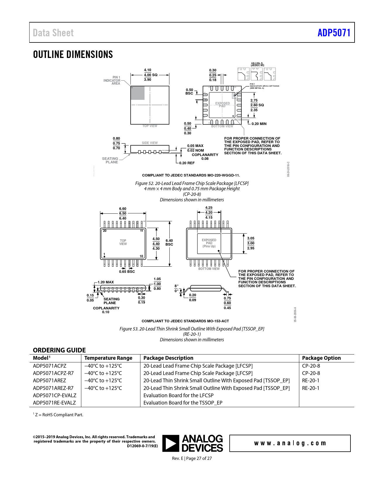
Data Sheet. ADP5071. OUTLINE DIMENSIONS. DETAIL A. (JEDEC 95). 4.10. 0.30. 4.00 SQ. 0.25. PIN 1. 3.90. INDICATOR. 0.18. AREA
33 предложений от 14 поставщиков Преобразователи постоянного тока в постоянный NO -40°C~+125°C@(TJ) 2 Adjustable 2.85V~15V LFCSP-20 Преобразователь DC-DC |
| ADP5071ACPZ
Analog Devices | от 114 ₽ | |
| ADP5071ACPZ-R7
Analog Devices | от 281 ₽ | |
| ADP5071ACPZ
Analog Devices | от 729 ₽ | |
| ADP5071ACPZ
Analog Devices | от 755 ₽ | |
Модельный ряд для этого даташита
Текстовая версия документа
Data Sheet ADP5071 OUTLINE DIMENSIONS DETAIL A (JEDEC 95) 4.10 0.30 4.00 SQ 0.25 PIN 1 3.90 INDICATOR 0.18 AREA P IN 1 IN D IC AT O R AR E A OP T IO N S 16 20 (SEE DETAIL A) 0.50 1 BSC 15 2.75 EXPOSED 2.60 SQ PAD 2.35 5 11 0.50 10 6 0.20 MIN TOP VIEW BOTTOM VIEW 0.40 0.30 0.80 FOR PROPER CONNECTION OF 0.75 SIDE VIEW THE EXPOSED PAD, REFER TO 0.05 MAX THE PIN CONFIGURATION AND 0.70 0.02 NOM FUNCTION DESCRIPTIONS SECTION OF THIS DATA SHEET. COPLANARITY SEATING 0.08 PLANE 0.20 REF C 2018- -003502 24- G K P COMPLIANT TO JEDEC STANDARDS MO-220-WGGD-11. 09-
Figure 52. 20-Lead Lead Frame Chip Scale Package [LFCSP] 4 mm × 4 mm Body and 0.75 mm Package Height (CP-20-8) Dimensions shown in millimeters
6.60 4.25 6.50 4.20 6.40 4.15 20 11 4.50 3.05 EXPOSED TOP 6.40 PAD VIEW 4.40 BSC 3.00 (Pins Up) 4.30 2.95 1 10 BOTTOM VIEW 0.65 BSC FOR PROPER CONNECTION OF THE EXPOSED PAD, REFER TO 1.05 THE PIN CONFIGURATION AND 1.20 MAX 1.00 FUNCTION DESCRIPTIONS 8° SECTION OF THIS DATA SHEET. 0.80 0° 0.15 0.20 0.30 0.75 0.05 SEATING 0.09 PLANE 0.19 0.60 0.45 A COPLANARITY 0.10 2006- 08- COMPLIANT TO JEDEC STANDARDS MO-153-ACT 05-
Figure 53. 20-Lead Thin Shrink Small Outline With Exposed Pad [TSSOP_EP] (RE-20-1) Dimensions shown in millimeters
ORDERING GUIDE Model1 Temperature Range Package Description Package Option
ADP5071ACPZ −40°C to +125°C 20-Lead Lead Frame Chip Scale Package [LFCSP] CP-20-8 ADP5071ACPZ-R7 −40°C to +125°C 20-Lead Lead Frame Chip Scale Package [LFCSP] CP-20-8 ADP5071AREZ −40°C to +125°C 20-Lead Thin Shrink Small Outline With Exposed Pad [TSSOP_EP] RE-20-1 ADP5071AREZ-R7 −40°C to +125°C 20-Lead Thin Shrink Small Outline With Exposed Pad [TSSOP_EP] RE-20-1 ADP5071CP-EVALZ Evaluation Board for the LFCSP ADP5071RE-EVALZ Evaluation Board for the TSSOP_EP 1 Z = RoHS Compliant Part.
©2015–2019 Analog Devices, Inc. All rights reserved. Trademarks and registered trademarks are the property of their respective owners. D12069-0-7/19(E)
Rev. E | Page 27 of 27 Document Outline Features Applications Typical Application Circuit General Description Revision History Specifications Absolute Maximum Ratings Thermal Resistance ESD Caution Pin Configurations and Function Descriptions Typical Performance Characteristics Theory of Operation PWM Mode PSM Mode Undervoltage Lockout (UVLO) Oscillator and Synchronization Internal Regulators Precision Enabling Soft Start Slew Rate Control Current-Limit Protection Overvoltage Protection Thermal Shutdown Start-Up Sequence Applications Information ADIsimPower Design Tool Component Selection Feedback Resistors Output Capacitors Input Capacitor VREG Capacitor VREF Capacitor Soft Start Resistor Diodes Inductor Selection for the Boost Regulator Inductor Selection for the Inverting Regulator Loop Compensation Boost Regulator Inverting Regulator Common Applications Super Low Noise With Optional LDOs SEPIC Step-Up/Step-Down Operation Layout Considerations Outline Dimensions Ordering Guide

 Купить ADP5071ACPZ на РадиоЛоцман.Цены — от 114 до 1 171 ₽


