Preliminary Datasheet SLG47105 (Dialog Semiconductor) - 209
| Производитель | Dialog Semiconductor |
| Описание | GreenPAK Programmable Mixed-Signal Matrix with High Voltage Features |
| Страниц / Страница | 223 / 209 — SLG47105. GreenPAK Programmable Mixed-Signal Matrix with High. … |
| Формат / Размер файла | PDF / 4.3 Мб |
| Язык документа | английский |
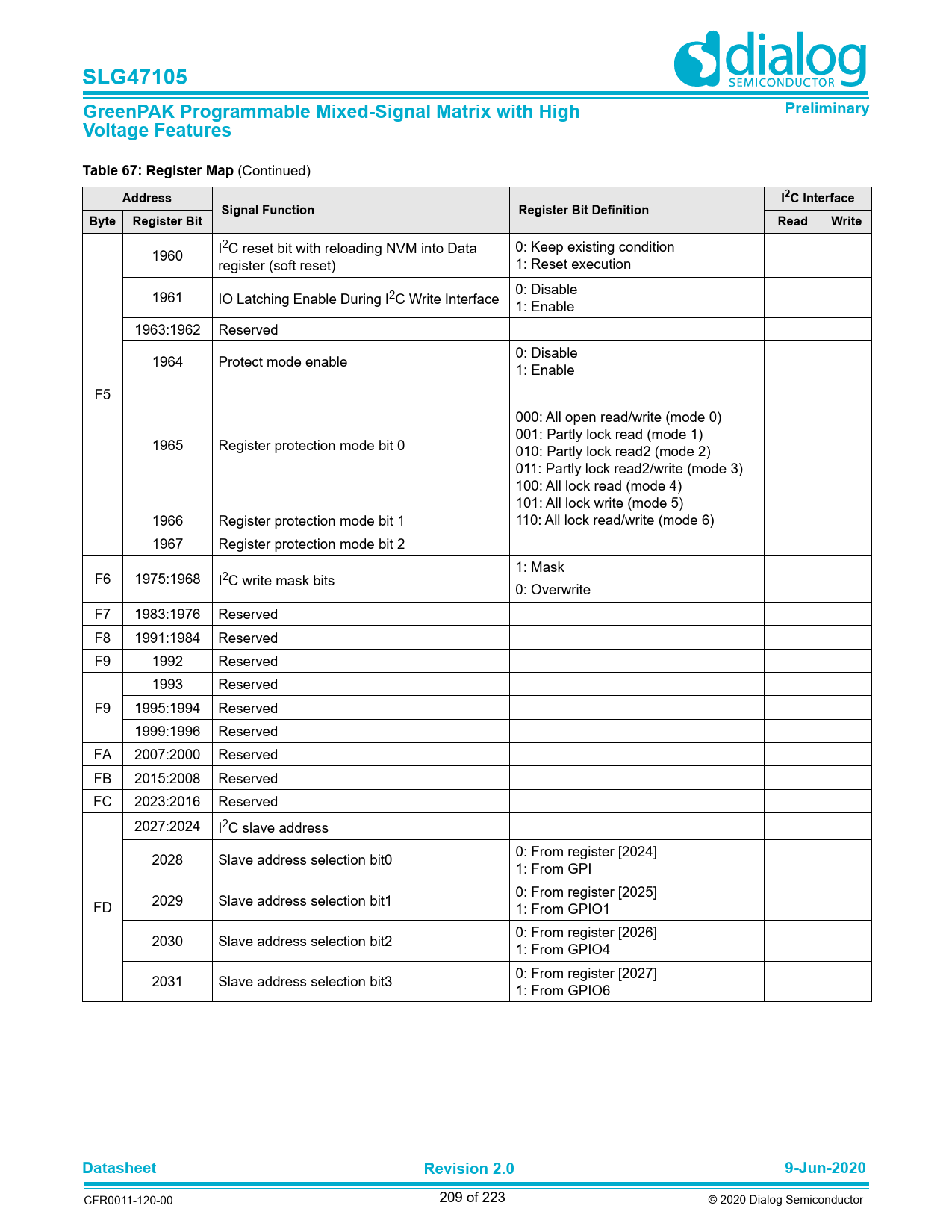
SLG47105. GreenPAK Programmable Mixed-Signal Matrix with High. Preliminary. Voltage Features. Table 67: Register Map. Address
Модельный ряд для этого даташита
Текстовая версия документа
SLG47105 GreenPAK Programmable Mixed-Signal Matrix with High Preliminary Voltage Features Table 67: Register Map
(Continued)
Address I2C Interface Signal Function Register Bit Definition Byte Register Bit Read Write
I2C reset bit with reloading NVM into Data 0: Keep existing condition 1960 register (soft reset) 1: Reset execution 0: Disable 1961 IO Latching Enable During I2C Write Interface 1: Enable 1963:1962 Reserved 0: Disable 1964 Protect mode enable 1: Enable F5 000: All open read/write (mode 0) 001: Partly lock read (mode 1) 1965 Register protection mode bit 0 010: Partly lock read2 (mode 2) 011: Partly lock read2/write (mode 3) 100: All lock read (mode 4) 101: All lock write (mode 5) 1966 Register protection mode bit 1 110: All lock read/write (mode 6) 1967 Register protection mode bit 2 1: Mask F6 1975:1968 I2C write mask bits 0: Overwrite F7 1983:1976 Reserved F8 1991:1984 Reserved F9 1992 Reserved 1993 Reserved F9 1995:1994 Reserved 1999:1996 Reserved FA 2007:2000 Reserved FB 2015:2008 Reserved FC 2023:2016 Reserved 2027:2024 I2C slave address 0: From register [2024] 2028 Slave address selection bit0 1: From GPI 0: From register [2025] 2029 Slave address selection bit1 FD 1: From GPIO1 0: From register [2026] 2030 Slave address selection bit2 1: From GPIO4 0: From register [2027] 2031 Slave address selection bit3 1: From GPIO6
Datasheet Revision 2.0 9-Jun-2020
CFR0011-120-00 209 of 223 © 2020 Dialog Semiconductor Document Outline General Description Key Features Applications 1 Block Diagram 2 Pinout 2.1 Pin Configuration - STQFN- 20L 3 Characteristics 3.1 Absolute Maximum Ratings 3.2 Electrostatic Discharge Ratings 3.3 Recommended Operating Conditions 3.4 Thermal Information 3.5 Electrical Characteristics 3.6 HV Output Electrical Characteristic 3.7 Protection Circuits Electrical Characteristic 3.8 Timing Characteristics 3.9 Counter/Delay Characteristics 3.10 Oscillator Characteristics 3.10.1 OSC Power-On Delay 3.11 Current Sense Comparator Characteristics 3.12 Differential Amplifier with Integrator and Comparator Characteristics 3.13 ACMP Characteristics 3.14 Analog Temperature Sensor Characteristics 4 User Programmability 5 System Overview 5.1 GPIO Pins 5.2 High Voltage Output Pins 5.3 Connection Matrix 5.4 Two Current Sense Comparators 5.5 Differential Amplifier with Integrator and Comparator 5.6 Two general purpose analog comparators 5.7 Voltage reference 5.8 Twelve Combination Function Macrocells 5.9 Five Multi-Function Macrocells 5.10 Two PWM Macrocells 5.11 Serial Communication 5.12 Programmable Delay 5.13 Additional Logic Function 5.14 Two Oscillators 5.15 Dual VDD 6 Input/Output Pins 6.1 GPIO Pins 6.2 GPI Pin 6.3 HV GPO Pins 6.4 Pull-Up/Down Resistors 6.5 Fast Pull-Up/Down during Power-Up 6.6 GPI IO Structure (for VDD Group) 6.6.1 GPI IO Structure 6.7 I2C Mode IO Structure (for VDD Group) 6.7.1 I2C Mode IO Structure (for SCL/GPIO2 and SDA/GPIO3, Register OE) 6.8 Matrix OE IO Structure (for VDD Group) 6.8.1 Matrix OE IO Structure (for GPIOs 0, 1, 4, 5, 6) 6.9 GPO Matrix OE Structure (For VDD2 Group) 6.9.1 GPO with Matrix OE Structure (for HV GPOs 0 and 1) 6.9.2 GPO with Matrix OE Structure (for HV GPOs 2 and 3) 7 High Voltage Output Modes 7.1 Full-Bridge Mode 7.2 Half bridge mode 7.3 Pre-Driver Mode 7.4 Parallel Connection of HV GPO 7.5 Protection Circuits 7.5.1 General FAULT signals 7.5.2 Advanced Current Control 7.5.3 Over-current Protection (OCP) 7.5.4 Thermal Shutdown (TSD) and Thermal Considerations 7.5.5 Under-voltage Lockout (UVLO) 7.6 PWM Voltage Control 8 Differential Amplifier with Integrator and Comparator 8.1 Differential Amplifier with Integrator Block Diagram 9 Current Sense Comparator 9.1 Current Sense Comparator0 Block Diagram 9.2 Current Sense Comparator1 Block Diagram 9.3 Current Regulation 10 Connection Matrix 10.1 Matrix Input Table 10.2 Matrix Output Table 10.3 Connection Matrix Virtual Inputs 10.4 Connection Matrix Virtual Outputs 11 Combination Function Macrocells 11.1 2-bit LUT or D Flip-Flop Macrocells 11.1.1 2-bit LUT or D Flip-Flop Macrocell Used as 2-bit LUT 11.1.2 Initial Polarity Operations 11.2 2-bit LUT or Programmable Pattern Generator 11.2.1 2-bit LUT or PGen Macrocell Used as 2-bit LUT 11.3 3-bit LUT or D Flip-Flop with Set/Reset Macrocells 11.3.1 3-bit LUT or D Flip-Flop Macrocells Used as 3-bit LUTs 11.3.2 Initial Polarity Operations 11.4 3-bit LUT or D Flip-Flop with Set/Reset Macrocell or PWM Chopper 11.4.1 3-bit LUT or D Flip-Flop or PWM Chopper Macrocells Used as 3-bit LUTs 11.4.2 PWM chopper 11.4.3 Initial Polarity Operations 11.5 3-bit LUT or Pipe Delay/Ripple Counter Macrocell 11.5.1 3-bit LUT or Pipe Delay Macrocells Used as 3-bit LUT 11.6 4-bit LUT or D Flip-Flop Macrocell 11.6.1 4-bit LUT Macrocell Used as 4-bit LUT 12 Multi-Function Macrocells 12.1 3-bit LUT or DFF/LATCH with 8-bit Counter/Delay Macrocells 12.1.1 3-bit LUT or 8-bit CNT/DLY Block Diagrams 12.1.2 3-bit LUT or CNT/DLYs Used as 3-bit LUTs 12.2 4-bit LUT or DFF/LATCH with 16-bit Counter/Delay Macrocell 12.2.1 4-bit LUT or DFF/LATCH with 16-bit CNT/DLY Block Diagram 12.2.2 4-bit LUT or 16-bit Counter/Delay Macrocells Used as 4-bit LUTs 12.3 CNT/DLY/FSM Timing Diagrams 12.3.1 Delay Mode CNT/DLY0 to CNT/DLY4 12.3.2 Count Mode (Count Data: 3), Counter Reset (Rising Edge Detect) CNT/DLY0 to CNT/DLY4 12.3.3 One-shot Mode CNT/DLY0 to CNT/DLY4 12.3.4 Frequency Detection Mode CNT/DLY0 to CNT/DLY4 12.3.5 Edge Detection Mode CNT/DLY1 to CNT/DLY4 12.3.6 Delayed Edge Detection Mode CNT/DLY0 to CNT/DLY4 12.3.7 CNT/FSM Mode CNT/DLY0 12.3.8 The Difference in Counter Value for Counter, Delay, One-Shot, and Frequency Detect Modes 12.4 Wake and Sleep Controller 13 Pulse Width Modulator Macrocell (PWM) 13.1 8-bit/7-bit PWM Resolution 13.2 PWM Inputs 13.3 PWM Outputs 13.4 I2C/Matrix/Auto dynamically changeable Duty Cycle and Period 13.5 I2C PWM Duty Cycle read/write 13.6 Flexible OSC-integrated Divider 13.7 Inverted Output option 13.8 Changeable dead band option for OUT+ and OUT- 13.9 Initial PWM value 13.10 Sync On/Off setting for Power-Down signal 13.11 Regular/Preset Registers Mode 13.12 PWM Continuous/Autostop mode 13.13 Internal Oscillator Auto Disable Mode 13.14 Phase Correct PWM Mode 13.15 PWM Period Output 13.16 PWM Block Diagrams 13.17 PWM Register Settings 14 Analog Comparators 14.1 ACMP0H Block Diagram 14.2 ACMP1H Block Diagram 14.3 ACMP Typical Performance 15 Programmable Delay/Edge Detector 15.1 Programmable Delay Timing Diagram - Edge Detector OUTPUT 16 Additional Logic Function. Deglitch Filter 17 Voltage Reference 17.1 Voltage Reference Overview 17.2 Vref Selection Table 17.3 Mode Selection 17.4 Vref Block Diagram 17.5 Vref Load Regulation 18 Clocking 18.1 OSC General description 18.2 Oscillator0 (2.048 kHz) 18.3 Oscillator1 (25 MHz) 18.4 CNT/DLY Clock Scheme 18.5 PWM Clock Scheme 18.6 External Clocking 18.6.1 GPIO1 Source for Oscillator0 (2.048 kHz) 18.6.2 GPIO4 Source for Oscillator 1 (25 MHz) 18.7 Oscillators Power-On Delay 19 Low Power Bandgap (LP_BG) 20 Power-On Reset 20.1 General Operation 20.2 POR Sequence 20.3 Macrocells Output States During POR Sequence 20.3.1 Initialization 20.3.2 Power-Down 21 I2C Serial Communications Macrocell 21.1 I2C Serial Communications Macrocell Overview 21.2 I2C Serial Communications Device Addressing 21.3 I2C Serial General Timing 21.4 I2C Serial Communications Commands 21.4.1 Byte Write Command 21.4.2 Sequential Write Command 21.4.3 Current Address Read Command 21.4.4 Random Read Command 21.4.5 Sequential Read Command 21.5 I2C Serial Command Register Map 21.5.1 Register Read/Write Protection 21.5.2 I2C Serial Reset Command 21.5.3 I2C Additional Options 21.5.4 Reading Current Counter Data via I2C 21.5.5 I2C Byte Write Bit Masking 22 Analog Temperature Sensor 23 Register Definitions 23.1 Register Map 24 Package Top Marking Definitions 24.1 STQFN 20L 2 mm x 3 mm 0.4P FCD Green 25 Package Information 25.1 Package Outlines for STQFN 20L 2 mm x 3 mm 0.4P FCD Green Package 25.2 Moisture Sensitivity Level 25.3 Soldering Information 26 Ordering Information 26.1 Tape and Reel Specifications 26.2 Carrier Tape Drawing and Dimensions 27 Thermal Guidelines 28 Layout consideration 29 Layout Guidelines 29.1 STQFN 20L 2 mm x 3.0 mm x 0.55 mm 0.4P FCD Package Glossary Revision History

 Купить SLG47105V на РадиоЛоцман.Цены — от 16 до 204 ₽

