Datasheet AD8250 (Analog Devices)
| Производитель | Analog Devices |
| Описание | 10 MHz G = 1, 2, 5, 10 iCMOS Programmable Gain Instrumentation Amplifier |
| Страниц / Страница | 25 / 1 — 10 MHz, 20 V/μs, G = 1, 2, 5, 10. CMOS. Programmable Gain Instrumentation … |
| Версия | C |
| Формат / Размер файла | PDF / 927 Кб |
| Язык документа | английский |
10 MHz, 20 V/μs, G = 1, 2, 5, 10. CMOS. Programmable Gain Instrumentation Amplifier. Data Sheet. AD8250. FEATURES
Текстовая версия документа
link to page 1
10 MHz, 20 V/μs, G = 1, 2, 5, 10
i
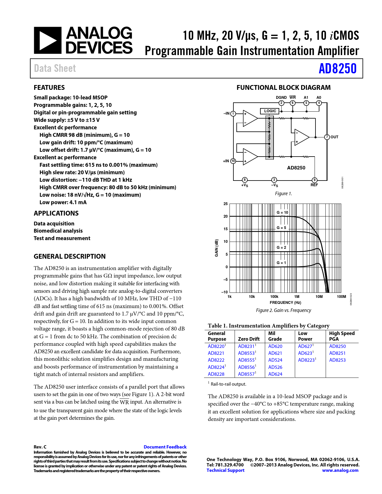
CMOS Programmable Gain Instrumentation Amplifier Data Sheet AD8250 FEATURES FUNCTIONAL BLOCK DIAGRAM Small package: 10-lead MSOP DGND WR A1 A0 Programmable gains: 1, 2, 5, 10 2 6 5 4 Digital or pin-programmable gain setting LOGIC –IN 1 Wide supply: ±5 V to ±15 V Excellent dc performance High CMRR 98 dB (minimum), G = 10 7 OUT Low gain drift: 10 ppm/°C (maximum) Low offset drift: 1.7 μV/°C (maximum), G = 10 Excellent ac performance +IN 10 Fast settling time: 615 ns to 0.001% (maximum) AD8250 High slew rate: 20 V/µs (minimum) Low distortion: −110 dB THD at 1 kHz 8 3 9
001
High CMRR over frequency: 80 dB to 50 kHz (minimum) +VS –VS REF
06288-
Low noise: 18 nV/√Hz, G = 10 (maximum)
Figure 1.
Low power: 4.1 mA 25 APPLICATIONS G = 10 20 Data acquisition Biomedical analysis 15 G = 5 Test and measurement B) 10 d N ( G = 2 GENERAL DESCRIPTION AI 5 G G = 1
The AD8250 is an instrumentation amplifier with digitally
0
programmable gains that has GΩ input impedance, low output noise, and low distortion making it suitable for interfacing with
–5
sensors and driving high sample rate analog-to-digital converters
–10
(ADCs). It has a high bandwidth of 10 MHz, low THD of −110
1k 10k 100k 1M 10M 100M
023 dB and fast settling time of 615 ns (maximum) to 0.001%. Offset
FREQUENCY (Hz)
06288- drift and gain drift are guaranteed to 1.7 μV/°C and 10 ppm/°C, Figure 2. Gain vs. Frequency respectively, for G = 10. In addition to its wide input common voltage range, it boasts a high common-mode rejection of 80 dB
Table 1. Instrumentation Amplifiers by Category
at G = 1 from dc to 50 kHz. The combination of precision dc
General Mil Low High Speed Purpose Zero Drift Grade Power PGA
performance coupled with high speed capabilities makes the AD82201 AD82311 AD620 AD6271 AD8250 AD8250 an excel ent candidate for data acquisition. Furthermore, AD8221 AD85531 AD621 AD6231 AD8251 this monolithic solution simplifies design and manufacturing AD8222 AD85551 AD524 AD82231 AD8253 and boosts performance of instrumentation by maintaining a AD82241 AD85561 AD526 tight match of internal resistors and amplifiers. AD8228 AD85571 AD624 1 The AD8250 user interface consists of a parallel port that allows Rail-to-rail output. users to set the gain in one of two ways (see Figure 1). A 2-bit word The AD8250 is available in a 10-lead MSOP package and is sent via a bus can be latched using the WR input. An alternative is specified over the −40°C to +85°C temperature range, making to use the transparent gain mode where the state of the logic levels it an excellent solution for applications where size and packing at the gain port determines the gain. density are important considerations.
Rev. C Document Feedback Information furnished by Analog Devices is believed to be accurate and reliable. However, no responsibility is assumed by Analog Devices for its use, nor for any infringements of patents or other rights of third parties that may result from its use. Specifications subject to change without notice. No One Technology Way, P.O. Box 9106, Norwood, MA 02062-9106, U.S.A. license is granted by implication or otherwise under any patent or patent rights of Analog Devices. Tel: 781.329.4700 ©2007–2013 Analog Devices, Inc. All rights reserved. Trademarks and registered trademarks are the property of their respective owners. Technical Support www.analog.com
Document Outline Features Applications General Description Functional Block Diagram Revision History Specifications Timing Diagram Absolute Maximum Ratings Maximum Power Dissipation ESD Caution Pin Configuration and Function Descriptions Typical Performance Characteristics Theory of Operation Gain Selection Transparent Gain Mode Latched Gain Mode Timing for Latched Gain Mode Power Supply Regulation and Bypassing Input Bias Current Return Path Input Protection Reference Terminal Common-Mode Input Voltage Range Layout Grounding Coupling Noise Common-Mode Rejection RF Interference Driving an ADC Applications Differential Output Setting Gains with a Microcontroller Data Acquisition Outline Dimensions Ordering Guide

 аккумуляторов")


