Datasheet AD7822, AD7825, AD7829 (Analog Devices)
| Производитель | Analog Devices |
| Описание | 3 V/5 V, 2 MSPS, 8-Bit, 1-/4-/8-Channel Sampling ADCs |
| Страниц / Страница | 28 / 1 — 3 V/5 V, 2 MSPS, 8-Bit, 1-/4-/8-Channel. Sampling ADCs. … |
| Версия | C |
| Формат / Размер файла | PDF / 531 Кб |
| Язык документа | английский |
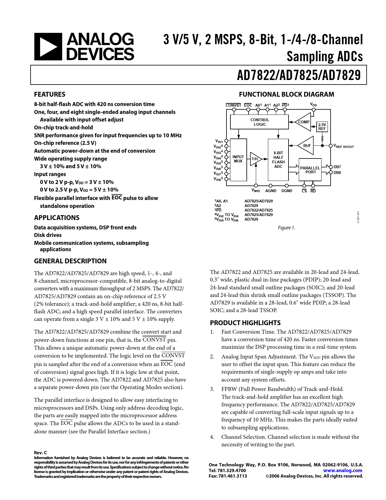
3 V/5 V, 2 MSPS, 8-Bit, 1-/4-/8-Channel. Sampling ADCs. AD7822/AD7825/AD7829. FEATURES. FUNCTIONAL BLOCK DIAGRAM
Модельный ряд для этого даташита
Текстовая версия документа
link to page 15 link to page 17
3 V/5 V, 2 MSPS, 8-Bit, 1-/4-/8-Channel Sampling ADCs AD7822/AD7825/AD7829 FEATURES FUNCTIONAL BLOCK DIAGRAM 8-bit half-flash ADC with 420 ns conversion time CONVST EOC A01 A11 A22 PD3 VDD One, four, and eight single-ended analog input channels Available with input offset adjust CONTROL COMP LOGIC 2.5V On-chip track-and-hold REF SNR performance given for input frequencies up to 10 MHz V On-chip reference (2.5 V) IN1 V 4 BUF VREF IN/OUT IN2 Automatic power-down at the end of conversion V 4 IN3 8-BIT 4 Wide operating supply range VIN4 INPUT T/H HALF V 5 MUX IN5 FLASH 3 V ± 10% and 5 V ± 10% V 5 ADC DB7 IN6 PARALLEL Input ranges 5 PORT V DB0 IN7 V 5 IN8 0 V to 2 V p-p, VDD = 3 V ± 10% 0 V to 2.5 V p-p, VDD = 5 V ± 10% VMID AGND DGND CS RD Flexible parallel interface with EOC pulse to allow 1A0, A1 AD7825/AD7829 standalone operation 2A2 AD7829 3PD AD7822/AD7825
1
4V
00
APPLICATIONS IN2 TO VIN4 AD7825/AD7829
1-
5VIN5 TO VIN8 AD7829
32 01
Data acquisition systems, DSP front ends
Figure 1.
Disk drives Mobile communication systems, subsampling applications GENERAL DESCRIPTION
The AD7822/AD7825/AD7829 are high speed, 1-, 4-, and The AD7822 and AD7825 are available in 20-lead and 24-lead, 8-channel, microprocessor-compatible, 8-bit analog-to-digital 0.3" wide, plastic dual in-line packages (PDIP); 20-lead and converters with a maximum throughput of 2 MSPS. The AD7822/ 24-lead standard small outline packages (SOIC); and 20-lead AD7825/AD7829 contain an on-chip reference of 2.5 V and 24-lead thin shrink small outline packages (TSSOP). The (2% tolerance); a track-and-hold amplifier; a 420 ns, 8-bit half- AD7829 is available in a 28-lead, 0.6" wide PDIP; a 28-lead flash ADC; and a high speed parallel interface. The converters SOIC; and a 28-lead TSSOP. can operate from a single 3 V ± 10% and 5 V ± 10% supply.
PRODUCT HIGHLIGHTS
The AD7822/AD7825/AD7829 combine the convert start and 1. Fast Conversion Time. The AD7822/AD7825/AD7829 power-down functions at one pin, that is, the CONVST pin. have a conversion time of 420 ns. Faster conversion times This allows a unique automatic power-down at the end of a maximize the DSP processing time in a real-time system. conversion to be implemented. The logic level on the CONVST 2. Analog Input Span Adjustment. The VMID pin allows the pin is sampled after the end of a conversion when an EOC (end user to offset the input span. This feature can reduce the of conversion) signal goes high. If it is logic low at that point, requirements of single-supply op amps and take into the ADC is powered down. The AD7822 and AD7825 also have account any system offsets. a separate power-down pin (see the Operating Modes section). 3. FPBW (Full Power Bandwidth) of Track-and-Hold. The track-and-hold amplifier has an excellent high The parallel interface is designed to allow easy interfacing to frequency performance. The AD7822/AD7825/AD7829 microprocessors and DSPs. Using only address decoding logic, are capable of converting full-scale input signals up to a the parts are easily mapped into the microprocessor address frequency of 10 MHz. This makes the parts ideally suited space. The EOC pulse allows the ADCs to be used in a stand- to subsampling applications. alone manner (see the Parallel Interface section.) 4. Channel Selection. Channel selection is made without the necessity of writing to the part.
Rev. C Information furnished by Analog Devices is believed to be accurate and reliable. However, no responsibility is assumed by Analog Devices for its use, nor for any infringements of patents or other One Technology Way, P.O. Box 9106, Norwood, MA 02062-9106, U.S.A. rights of third parties that may result from its use. Specifications subject to change without notice. No license is granted by implication or otherwise under any patent or patent rights of Analog Devices. Tel: 781.329.4700 www.analog.com Trademarks and registered trademarks are the property of their respective owners. Fax: 781.461.3113 ©2006 Analog Devices, Inc. All rights reserved.
Document Outline FEATURES APPLICATIONS GENERAL DESCRIPTION FUNCTIONAL BLOCK DIAGRAM PRODUCT HIGHLIGHTS TABLE OF CONTENTS REVISION HISTORY SPECIFICATIONS TIMING CHARACTERISTICS TIMING DIAGRAM ABSOLUTE MAXIMUM RATINGS ESD CAUTION PIN CONFIGURATIONS AND FUNCTION DESCRIPTIONS TERMINOLOGY CIRCUIT INFORMATION CIRCUIT DESCRIPTION TYPICAL CONNECTION DIAGRAM ADC TRANSFER FUNCTION ANALOG INPUT POWER-UP TIMES POWER VS. THROUGHPUT OPERATING MODES PARALLEL INTERFACE MICROPROCESSOR INTERFACING AD7822/AD7825/AD7829 TO 8051 AD7822/AD7825/AD7829 TO PIC16C6x/PIC16C7x AD7822/AD7825/AD7829 TO ADSP-21xx INTERFACING MULTIPLEXER ADDRESS INPUTS AD7822 STANDALONE OPERATION OUTLINE DIMENSIONS ORDERING GUIDE

 аккумуляторов")


