
Datasheet Microchip MDB1900ZC — Даташит
| Производитель | Microchip |
| Серия | MDB1900ZC |
MDB1900ZC — это буфер с нулевой задержкой и полностью интегрированной высокопроизводительной, маломощной и малошумящей программируемой схемой ФАПЧ.
Datasheets
MDB1900ZB - Zero Delay Buffer for PCIe, SAS, SATA, ESI, and QPI
PDF, 1.0 Мб, Файл опубликован: 9 ноя 2015
Выписка из документа
MDB1900ZC - Zero Delay Buffer for PCIe, SAS, SATA, ESI, and QPI
PDF, 980 Кб, Файл опубликован: 9 ноя 2015
Выписка из документа
| MDB1900ZC Micrel | от 226 ₽ | ||
| MDB1900ZC Micrel | от 226 ₽ | ||
| MDB1900ZC Microchip | по запросу | ||
 Купить MDB1900ZC на РадиоЛоцман.Цены

Статус
| MDB1900ZCQY | MDB1900ZCQY-TR | MDB1900ZCQZ | MDB1900ZCQZ-TR | |
|---|---|---|---|---|
| Статус продукта | В производстве (Подходит для новых разработок, но могут существовать и более новые альтернативы) | В производстве (Подходит для новых разработок, но могут существовать и более новые альтернативы) | В производстве (Подходит для новых разработок, но могут существовать и более новые альтернативы) | В производстве (Подходит для новых разработок, но могут существовать и более новые альтернативы) |
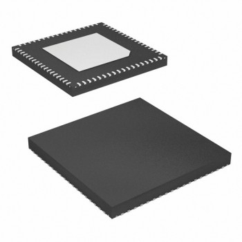
Корпус / Упаковка / Маркировка
| MDB1900ZCQY | MDB1900ZCQY-TR | MDB1900ZCQZ | MDB1900ZCQZ-TR | |
|---|---|---|---|---|
| N | 1 | 2 | 3 | 4 |
| Корпус | VQFN | VQFN | VQFN | VQFN |
| Количество выводов | 72 | 72 | 72 | 72 |
Параметры
| Parameters / Models | MDB1900ZCQY | MDB1900ZCQY-TR | MDB1900ZCQZ | MDB1900ZCQZ-TR |
|---|---|---|---|---|
| No. of Outputs | 19 | 19 | 19 | 19 |
Экологический статус
| MDB1900ZCQY | MDB1900ZCQY-TR | MDB1900ZCQZ | MDB1900ZCQZ-TR | |
|---|---|---|---|---|
| RoHS | Совместим | Совместим | Совместим | Совместим |
Другие варианты исполнения
Модельный ряд
Серия: MDB1900ZC (4)
Классификация производителя
- Clock and Timing > Clock and Data Distribution > Zero Delay Buffers PCIe Buffers


