Datasheet MP6925A (Monolithic Power Systems) - 13
| Производитель | Monolithic Power Systems |
| Описание | Fast Turn-Off, CCM/DCM Compatible, Dual-LLC, Synchronous Rectifier with lmproved Noise Immunity |
| Страниц / Страница | 15 / 13 — MP6925A – FAST TURN-OFF, CCM/DCM DUAL LLC SYNCHRONOUS RECTIFIER. PCB … |
| Формат / Размер файла | PDF / 1.3 Мб |
| Язык документа | английский |
MP6925A – FAST TURN-OFF, CCM/DCM DUAL LLC SYNCHRONOUS RECTIFIER. PCB Layout Guidelines. System Power Loop. Sensing for VD/VS

23 предложений от 8 поставщиков Микросхема: FAST TURN-OFF, CCM/DCM COMPATIBL |
| MP6925AGS-Z
| от 67 ₽ | |
| MP6925AGS-P
Monolithic Power Systems | 143 ₽ | |
| MP6925AGS-Z
Monolithic Power Systems | 151 ₽ | |
| MP6925AGS-Z
Monolithic Power Systems | от 160 ₽ | |
Модельный ряд для этого даташита
Текстовая версия документа
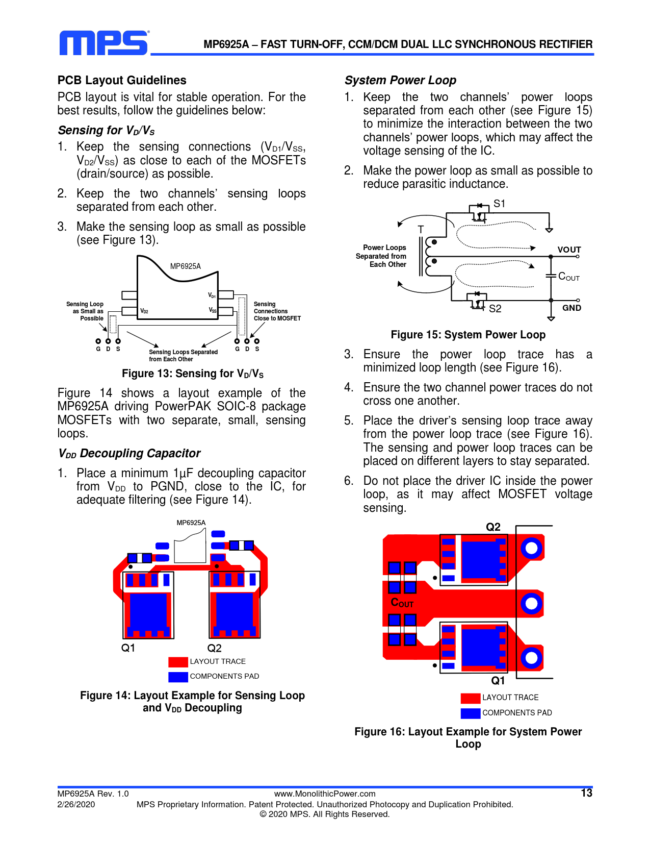
MP6925A – FAST TURN-OFF, CCM/DCM DUAL LLC SYNCHRONOUS RECTIFIER PCB Layout Guidelines System Power Loop
PCB layout is vital for stable operation. For the 1. Keep the two channels’ power loops best results, follow the guidelines below: separated from each other (see Figure 15) to minimize the interaction between the two
Sensing for VD/VS
channels’ power loops, which may affect the 1. Keep the sensing connections (VD1/VSS, voltage sensing of the IC. VD2/VSS) as close to each of the MOSFETs (drain/source) as possible. 2. Make the power loop as small as possible to reduce parasitic inductance. 2. Keep the two channels’ sensing loops separated from each other. S1 3. Make the sensing loop as small as possible T (see Figure 13).
Power Loops VOUT Separated from
MP6925A
Each Other
COUT
VD1 Sensing Loop Sensing GND as Small as V V
S2
D2 SS Connections Possible Close to MOSFET Figure 15: System Power Loop G D S G D S Sensing Loops Separated
3. Ensure the power loop trace has a
from Each Other
minimized loop length (see Figure 16).
Figure 13: Sensing for VD/VS
4. Ensure the two channel power traces do not Figure 14 shows a layout example of the cross one another. MP6925A driving PowerPAK SOIC-8 package MOSFETs with two separate, small, sensing 5. Place the driver’s sensing loop trace away loops. from the power loop trace (see Figure 16). The sensing and power loop traces can be
VDD Decoupling Capacitor
placed on different layers to stay separated. 1. Place a minimum 1µF decoupling capacitor 6. Do not place the driver IC inside the power from VDD to PGND, close to the IC, for loop, as it may affect MOSFET voltage adequate filtering (see Figure 14). sensing. MP6925A
Q2 COUT
Q1 Q2 LAYOUT TRACE COMPONENTS PAD
Q1 Figure 14: Layout Example for Sensing Loop
LAYOUT TRACE
and VDD Decoupling
COMPONENTS PAD
Figure 16: Layout Example for System Power Loop
MP6925A Rev. 1.0 www.MonolithicPower.com
13
2/26/2020 MPS Proprietary Information. Patent Protected. Unauthorized Photocopy and Duplication Prohibited. © 2020 MPS. All Rights Reserved.

 Купить MP6925AGS на РадиоЛоцман.Цены — от 39 до 160 ₽